SLVS292F June 2000 – September 2019 TPS3836 , TPS3837 , TPS3838
PRODUCTION DATA.
- 1 Features
- 2 Applications
- 3 Description
- 4 Revision History
- 5 Device Comparison Table
- 6 Pin Configuration and Functions
- 7 Specifications
- 8 Parameter Measurement Information
- 9 Detailed Description
- 10Application and Implementation
- 11Power Supply Recommendations
- 12Layout
- 13Device and Documentation Support
- 14Mechanical, Packaging, and Orderable Information
封装选项
请参考 PDF 数据表获取器件具体的封装图。
机械数据 (封装 | 引脚)
- DBV|5
- DRV|6
散热焊盘机械数据 (封装 | 引脚)
- DRV|6
订购信息
6 Pin Configuration and Functions
TPS3838 DRV Package
6-Pin WSON
(Top View)

1. N/C: Not Connected
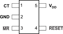
TPS3836 and TPS3838 DBV Package
5-Pin SOT
(Top View)

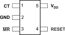
TPS3837 DBV Package
5-Pin SOT
(Top View)

Pin Functions
| PIN | I/O | DESCRIPTION | |||
|---|---|---|---|---|---|
| NAME | NO. | ||||
| WSON | SOT (TPS3836, TPS3838) | SOT (TPS3837) | |||
| CT | 6 | 1 | 1 | — | Capacitor Time Delay Pin. Connect this pin to GND to set reset delay time to 10 ms. Connect this pin to VDD to set reset delay time to 200 ms. |
| GND | 2 | 2 | 2 | — | Ground |
| MR | 4 | 3 | 3 | I | Manual Reset. When MR activates to logic low, RESET/RESET activates. When MR is inactive, RESET/RESET depends only on the voltage at VDD. If MR is unused, connect to VDD to minimize current consumption. |
| N/C | 5 | — | — | — | No Connect |
| RESET | 3 | 4 | — | O | Active-Low Output Reset. When VDD falls below VIT or when MR activates to logic low, the RESET pin activates to logic low. When VDD rises above VIT plus VHYS and MR deactivates to logic high, RESET deactivates to logic high after reset delay time tD. |
| RESET | — | — | 4 | O | Active-High Output Reset. When VDD falls below VIT or when MR activates to logic low, the RESET pin activates to logic high. When VDD rises above VIT plus VHYS and MR deactivates to logic high, RESET deactivates to logic low after reset delay time tD. |
| VDD | 1 | 5 | 5 | I | Input Supply Voltage. This device monitors the voltage at the VDD pin. |