SLVS363G August   2001  – September 2016 TPS3103 , TPS3106 , TPS3110

PRODUCTION DATA.  

  1. Features
  2. Applications
  3. Description
  4. Revision History
  5. Available Options
  6. Pin Configuration and Functions
  7. Specifications
    1. 7.1 Absolute Maximum Ratings
    2. 7.2 ESD Ratings
    3. 7.3 Recommended Operating Conditions
    4. 7.4 Thermal Information
    5. 7.5 Electrical Characteristics
    6. 7.6 Timing Requirements
    7. 7.7 Switching Characteristics
    8. 7.8 Typical Characteristics
  8. Detailed Description
    1. 8.1 Overview
    2. 8.2 Functional Block Diagrams
    3. 8.3 Feature Description
      1. 8.3.1 Watchdog
      2. 8.3.2 Manual Reset (MR)
      3. 8.3.3 PFI, PFO
      4. 8.3.4 SENSE
    4. 8.4 Device Functional Modes
  9. Application and Implementation
    1. 9.1 Application Information
    2. 9.2 Typical Application
      1. 9.2.1 Design Requirements
      2. 9.2.2 Detailed Design Procedure
      3. 9.2.3 Application Curve
  10. 10Power Supply Recommendations
  11. 11Layout
    1. 11.1 Layout Guidelines
    2. 11.2 Layout Example
  12. 12Device and Documentation Support
    1. 12.1 Device Support
      1. 12.1.1 Development Support
        1. 12.1.1.1 Spice Models
      2. 12.1.2 Device Nomenclature
    2. 12.2 Related Links
    3. 12.3 Receiving Notification of Documentation Updates
    4. 12.4 Community Resources
    5. 12.5 Trademarks
    6. 12.6 Electrostatic Discharge Caution
    7. 12.7 Glossary
  13. 13Mechanical, Packaging, and Orderable Information

封装选项

请参考 PDF 数据表获取器件具体的封装图。

机械数据 (封装 | 引脚)
  • DBV|6
散热焊盘机械数据 (封装 | 引脚)
订购信息

6 Pin Configuration and Functions

TPS3103 DBV Package
6-Pin SOT-23
Top View
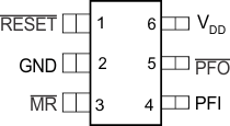
TPS3103 TPS3106 TPS3110 tps3103_po-lvs363.gif
TPS3106 DBV Package
6-Pin SOT-23
Top View
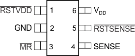
TPS3103 TPS3106 TPS3110 tps3106_po-lvs363.gif
TPS3110 DBV Package
6-Pin SOT-23
Top View
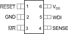
TPS3103 TPS3106 TPS3110 tps3110_po-lvs363.gif

Pin Functions

PIN I/O DESCRIPTION
NAME TPS3103 TPS3106 TPS3110
GND 2 2 2 GND
MR 3 3 3 I Manual-reset input. Pull low to force a reset. RESET remains low as long as MR is low and for the time-out period after MR goes high. Leave unconnected or connect to VDD when unused.
PFI 4 I Power-fail input compares to 0.551 V with no additional delay. Connect to VDD if not used.
PFO 5 O Power-fail output. Goes high when voltage at PFI rises above 0.551 V.
RESET 1 1 O Active-low reset output. Either push-pull or open-drain output stage.
RSTSENSE 5 O Active-low reset output. Logic level at RSTSENSE only depends on the voltage at SENSE and the status of MR.
RSTVDD 1 O Active-low reset output. Logic level at RSTVDD only depends on the voltage at VDD and the status of MR.
SENSE 4 4 I A reset is asserted if the voltage at SENSE is lower than 0.551 V. Connect to VDD if unused.
VDD 6 6 6 I Supply voltage. Powers the device and monitors its own voltage.
WDI 5 I Watchdog timer input. If WDI remains high or low longer than the time-out period, then reset is triggered. The timer clears when reset is asserted or when WDI sees a rising edge or a falling edge.