ZHCSLZ4D May 2020 – September 2021 TPS25850-Q1 , TPS25851-Q1 , TPS25852-Q1
PRODUCTION DATA
- 1 特性
- 2 应用
- 3 说明
- 4 Revision History
- 5 说明(续)
- 6 Device Comparison Table
- 7 Pin Configuration and Functions
- 8 Specifications
- 9 Parameter Measurement Information
-
10Detailed Description
- 10.1 Overview
- 10.2 Functional Block Diagram
- 10.3
Feature Description
- 10.3.1 Power-Down or Undervoltage Lockout
- 10.3.2 Input Overvoltage Protection (OVP) - Continuously Monitored
- 10.3.3 Buck Converter
- 10.3.4 FREQ/SYNC
- 10.3.5 Bootstrap Voltage (BOOT)
- 10.3.6 Minimum ON-Time, Minimum OFF-Time
- 10.3.7 Internal Compensation
- 10.3.8 Selectable Output Voltage (VSET)
- 10.3.9 Current Limit and Short Circuit Protection
- 10.3.10 Cable Compensation
- 10.3.11 Thermal Management With Temperature Sensing (TS) and OTSD
- 10.3.12 Thermal Shutdown
- 10.3.13 USB Enable On/Off Control (TPS25852-Q1)
- 10.3.14 FAULT Indication (TPS25851-Q1 and TPS25852-Q1)
- 10.3.15 USB Specification Overview
- 10.3.16 USB Type-C® Basics
- 10.3.17 USB Port Operating Modes
- 10.4 Device Functional Modes
- 11Application and Implementation
- 12Power Supply Recommendations
- 13Layout
- 14Device and Documentation Support
- 15Mechanical, Packaging, and Orderable Information
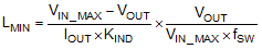
11.2.2.3 Inductor Selection
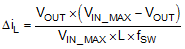
The most critical parameters for the inductor are the inductance, saturation current, and the rated current. The inductance is based on the desired peak-to-peak ripple current, ΔiL. Because the ripple current increases with the input voltage, the maximum input voltage is always used to calculate the minimum inductance LMIN. Use Equation 12 to calculate the minimum value of the output inductor. KIND is a coefficient that represents the amount of inductor ripple current relative to the maximum output current of the device. A reasonable value of KIND must be 20% to 40%. Note that when selecting the ripple current for applications with much smaller maximum load than the maximum available from the device, the maximum device current must still be used. During an instantaneous short or overcurrent operation event, the RMS and peak inductor current can be high. The inductor current rating must be higher than the current limit of the device.
In general, Choose lower inductance in switching power supplies because it usually corresponds to faster transient response, smaller DCR, and reduced size for more compact designs. Too low of an inductance can generate too large of an inductor current ripple such that overcurrent protection at the full load can be falsely triggered. Too low of an inductance also generates more conduction loss and inductor core loss. Larger inductor current ripple also implies larger output voltage ripple with the same output capacitors. With peak current mode control, TI does not recommend to have too small of an inductor current ripple. A larger peak current ripple improves the comparator signal to noise ratio.
For this design example, choose KIND = 0.3, and find an inductance of approximately 0.682 µH. Select the next standard value of 0.68 μH.