ZHCSEM7 December 2015 TPS2559-Q1
PRODUCTION DATA.
- 1 特性
- 2 应用
- 3 说明
- 4 修订历史记录
- 5 Device Comparison Table
- 6 Pin Configuration and Functions
- 7 Specifications
- 8 Parameter Measurement Information
- 9 Detailed Description
-
10Application and Implementation
- 10.1 Application Information
- 10.2
Typical Application
- 10.2.1 Design Requirements
- 10.2.2
Detailed Design Procedure
- 10.2.2.1 Step by Step Design Procedure
- 10.2.2.2 Input and Output Capacitance
- 10.2.2.3 Programming the Current-Limit Threshold
- 10.2.2.4 Design Above a Minimum Current Limit
- 10.2.2.5 Design Below a Maximum Current Limit
- 10.2.2.6 Accounting for Resistor Tolerance
- 10.2.2.7 Power Dissipation and Junction Temperature
- 10.2.2.8 Auto-Retry
- 10.2.2.9 Two-level Current-limit
- 10.2.3 Application Curves
- 11Power Supply Recommendations
- 12Layout
- 13器件和文档支持
- 14机械、封装和可订购信息
12 Layout
12.1 Layout Guidelines
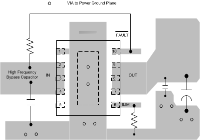
- Place the 100-nF bypass capacitor near the IN and GND pins, and make the connections using a low-inductance trace.
- Placing a high-value electrolytic capacitor and a 100-nF bypass capacitor on the output pin is recommended when large transient currents are expected on the output.
- The traces routing the RILIM resistor to the device should be as short as possible to reduce parasitic effects on the current limit accuracy.
- The PowerPAD should be directly connected to PCB ground plane using wide and short copper trace.
12.2 Layout Example
 Figure 31. TPS2559-Q1 Board Layout