ZHCSHL4I October 2008 – December 2017 TPS23754 , TPS23754-1 , TPS23756
PRODUCTION DATA.
- 1 特性
- 2 应用
- 3 说明
- 4 修订历史记录
- 5 Pin Configuration and Functions
- 6 Specifications
-
7 Detailed Description
- 7.1 Overview
- 7.2 Functional Block Diagram
- 7.3 Feature Description
- 7.4
Device Functional Modes
- 7.4.1
PoE Overview
- 7.4.1.1 Threshold Voltages
- 7.4.1.2 PoE Start-Up Sequence
- 7.4.1.3 Detection
- 7.4.1.4 Hardware Classification
- 7.4.1.5 Inrush and Start-Up
- 7.4.1.6 Maintain Power Signature
- 7.4.1.7 Start-Up and Converter Operation
- 7.4.1.8 PD Hotswap Operation
- 7.4.1.9 Converter Controller Features
- 7.4.1.10 Bootstrap Topology
- 7.4.1.11 Current Slope Compensation and Current Limit
- 7.4.1.12 Blanking – RBLNK
- 7.4.1.13 Dead Time
- 7.4.1.14 FRS and Synchronization
- 7.4.1.15 T2P, Start-Up, and Power Management
- 7.4.1.16 Thermal Shutdown
- 7.4.1.17 Adapter ORing
- 7.4.1.18 PPD ORing Features
- 7.4.1.19 Using DEN to Disable PoE
- 7.4.1.20 ORing Challenges
- 7.4.1
PoE Overview
-
8 Application and Implementation
- 8.1 Application Information
- 8.2
Typical Application
- 8.2.1 Design Requirements
- 8.2.2
Detailed Design Procedure
- 8.2.2.1 Input Bridges and Schottky Diodes
- 8.2.2.2 Protection, D1
- 8.2.2.3 Capacitor, C1
- 8.2.2.4 Detection Resistor, RDEN
- 8.2.2.5 Classification Resistor, RCLS
- 8.2.2.6 Dead Time Resistor, RDT
- 8.2.2.7 Switching Transformer Considerations and RVC
- 8.2.2.8 Special Switching MOSFET Considerations
- 8.2.2.9 Thermal Considerations and OTSD
- 8.2.2.10 APD Pin Divider Network, RAPD1, RAPD2
- 8.2.2.11 PPD Pin Divider Network, RPPD1, RPPD2
- 8.2.2.12 Setting Frequency (RFRS) and Synchronization
- 8.2.2.13 Current Slope Compensation
- 8.2.2.14 Blanking Period, RBLNK
- 8.2.2.15 Estimating Bias Supply Requirements and CVC
- 8.2.2.16 T2P Pin Interface
- 8.2.2.17 Advanced ORing Techniques
- 8.2.2.18 Soft Start
- 8.2.2.19 Frequency Dithering for Conducted Emissions Control
- 8.2.3 Application Curves
- 9 Power Supply Recommendations
- 10Layout
- 11器件和文档支持
- 12机械、封装和可订购信息
封装选项
请参考 PDF 数据表获取器件具体的封装图。
机械数据 (封装 | 引脚)
- PWP|20
散热焊盘机械数据 (封装 | 引脚)
- PWP|20
订购信息
8.2.2.13 Current Slope Compensation
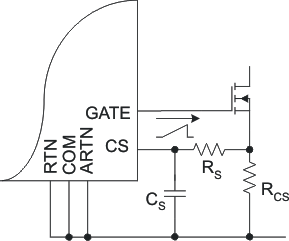
The TPS23754 device provides a fixed internal compensation ramp that suffices for most applications. RS (see Figure 31) may be used if the internally provided slope compensation is not enough.
Most current-mode control papers and application notes define the slope values in terms of VPP / TS (peak ramp voltage / switching period). However, the electrical characteristics table specifies the slope peak (VSLOPE) based on the maximum (78%) duty cycle. Assuming that the desired slope, VSLOPE-D (in mV/period), is based on the full period, compute RS per the following equation where VSLOPE, DMAX, and ISL-EX are from the electrical characteristics table with voltages in mV, current in μA, and the duty cycle is unitless (for example, DMAX = 0.78).

 Figure 31. Additional Slope Compensation
CS may be required if the presence of RS causes increased noise, due to adjacent signals like the gate drive, to appear at the CS pin.