ZHCSCV5B August 2014 – September 2014 TPS22994
PRODUCTION DATA.
- 1 特性
- 2 应用
- 3 说明
- 4 简化电路原理图
- 5 修订历史记录
- 6 Device Comparison Table
- 7 Pin Configuration and Functions
- 8 Specifications
-
9 Detailed Description
- 9.1 Overview
- 9.2 Functional Block Diagram
- 9.3
Feature Description
- 9.3.1 Operating Frequency
- 9.3.2 SDA/SCL Pin Configuration
- 9.3.3 Address (ADDx) Pin Configuration
- 9.3.4 On-Delay Control
- 9.3.5 Slew Rate Control
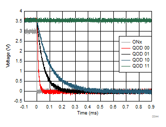
- 9.3.6 Quick Output Discharge (QOD) Control
- 9.3.7 Mode Registers
- 9.3.8 SwitchALL™ Command
- 9.3.9 VDD Supply For I2C Operation
- 9.3.10 Input Capacitor (Optional)
- 9.3.11 Output Capacitor (Optional)
- 9.3.12 I2C Protocol
- 9.4 Device Functional Modes
- 9.5 Register Map
-
10Applications and Implementation
- 10.1 Application Information
- 10.2 Typical Application
- 11Layout
- 12器件和文档支持
- 13机械封装和可订购信息
10 Applications and Implementation
NOTE
Information in the following applications sections is not part of the TI component specification, and TI does not warrant its accuracy or completeness. TI’s customers are responsible for determining suitability of components for their purposes. Customers should validate and test their design implementation to confirm system functionality.
10.1 Application Information
This section will cover applications of I2C in the TPS22994. Registers discussed here are specific to the TPS22994.
10.1.1 Input Capacitor (Optional)
To limit the voltage drop on the input supply caused by transient in-rush currents when the switch turns on into a discharged load capacitor or short-circuit, a capacitor needs to be placed between VIN and GND. A 1-µF ceramic capacitor, CIN, placed close to the pins, is usually sufficient. Higher values of CIN can be used to further reduce the voltage drop during high-current application. When switching heavy loads, it is recommended to have an input capacitor about 10 times higher than the output capacitor to avoid excessive voltage drop. For the fastest slew rate setting of the device, a CIN to CL ratio of at least 100 to 1 is recommended to avoid excessive voltage drop.
10.1.2 Output Capacitor (Optional)
Due to the integrated body diode of the NMOS switch, a CIN greater than CL is highly recommended. A CL greater than CIN can cause VOUT to exceed VIN when the system supply is removed. This could result in current flow through the body diode from VOUT to VIN. A CIN to CL ratio of at least 10 to 1 is recommended for minimizing VIN dip caused by inrush currents during startup. For the fastest slew rate setting of the device, a CIN to CL ratio of at least 100 to 1 is recommended to minimize VIN dip caused by inrush currents during startup.
10.1.3 Switch from GPIO Control to I2C Control (and vice versa)
The TPS22994 can be switched from GPIO control to I2C (and vice versa) mode by writing to the control register of the device. Each device has a single control register and is located at register address 05h. The register’s composition is as follows:
| Control register (Address: 05h) |
| BIT | B7 | B6 | B5 | B4 | B3 | B2 | B1 | B0 |
|---|---|---|---|---|---|---|---|---|
| DESCRIPTION | GPIO/I2C CH 4 | GPIO/I2C CH 3 | GPIO/I2C CH 2 | GPIO/I2C CH 1 | ENABLE CH 4 | ENABLE CH 3 | ENABLE CH 2 | ENABLE CH 1 |
| DEFAULT | 0 | 0 | 0 | 0 | 0 | 0 | 0 | 0 |
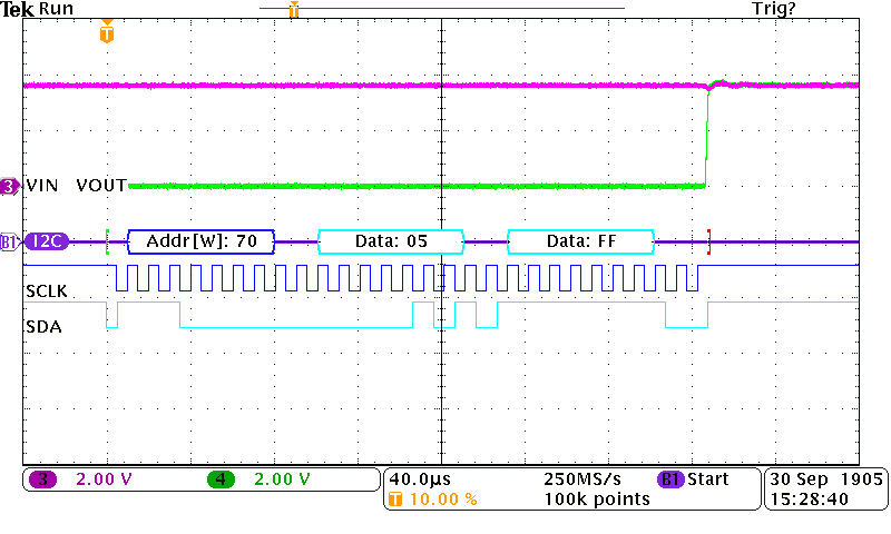
The higher four bits of the control register dictates if the device is in GPIO control (bit set to ‘0’) or I2C control (bit set to ‘1’). The transition from GPIO control to I2C control can be made with a single write command to the control register. See Figure 44 for the composition of a single write command. It is recommended that the channel of interest is transitioned from GPIO control to I2C control with the first write command and followed by a second write command to enable the channel via I2C control. This will ensure a smooth transition from GPIO control to I2C control.
10.1.4 Configuration of Configuration Registers
The TPS22994 contains four configuration registers (one for each channel) and are located at register addresses 01h through 04h. The register’s composition is as follows (single channel shown for clarity):
| Channel 1 configuration register (Address: 01h) |
| BIT | B7 | B6 | B5 | B4 | B3 | B2 | B1 | B0 |
|---|---|---|---|---|---|---|---|---|
| DESCRIPTION | X | ON-DELAY | SLEW RATE | QUICK OUTPUT DISCHARGE | ||||
| DEFAULT | X | 0 | 0 | 0 | 1 | 0 | 1 | 0 |
10.1.4.1 Single Register Configuration
A single configuration register can be written to using the write command sequence shown in Figure 44.
Multiple register writes to non-consecutive registers is treated as multiple single register writes and follows the same write command as that of a single register write as shown in Figure 44.
10.1.4.2 Multi-register Configuration (Consecutive Registers)
Multiple consecutive configuration registers can be written to using the write command sequence shown in Figure 45.
10.1.5 Configuration of Mode Registers
The TPS22994 contains twelve mode registers located at register addresses 06h through 11h. These mode registers allow the user to turn-on or turn-off multiple channels in a single TPS22994 or multiple channels spanning multiple TPS22994 devices with a single SwitchALLTM command.
For example, an application may have multiple power states (e.g. sleep, active, idle, etc.) as shown in Figure 51.
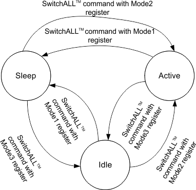 Figure 51. Application Example of Power States
In each of the different power states, different combinations of channels may be on or off. Each power state may be associated with a single mode register (Mode1, Mode2, etc.) across multiple TPS22994 as shown in Table 2. For example, with 7 quad-channel devices, up to 28 rails can be enabled/disabled with a single SwitchALLTM command.
Table 2. Application Example of State of Each Channel in Multiple TPS22994 in Different Power States
| Mode Register | Power State | Load Switch #1 | Load Switch #2 | Load Switch #N | |||||||||
|---|---|---|---|---|---|---|---|---|---|---|---|---|---|
| Ch. 1 | Ch. 2 | Ch. 3 | Ch. 4 | Ch. 1 | Ch. 2 | Ch. 3 | Ch. 4 | Ch. 1 | Ch. 2 | Ch. 3 | Ch. 4 | ||
| Mode1 | Sleep | Off | Off | Off | Off | Off | Off | Off | Off | Off | Off | Off | Off |
| Mode2 | Active | On | On | On | On | On | Off | On | Off | On | Off | On | Off |
| Mode3 | Idle | On | Off | On | Off | On | On | On | On | On | On | On | On |
The contents of the lower four bits of the mode register is copied into the lower four bits of the control register during an SwitchALLTM command. The address of the mode register to be copied is specified in the SwitchALLTM command (see Figure 48 for the structure of the SwitchALLTM command). By executing a SwitchALLTM command, the application will apply the different on/off combinations for the various power states with a single command rather than having to turn on/off each channel individually by re-configuring the control register. This reduces the latency and allows the application to control multiple channels synchronously. The example above shows the application using three mode registers, but the TPS22994 contains twelve mode registers, allowing for up to twelve power states.
The mode register’s composition is as follows (single mode register shown for clarity):
| Mode1 (Address: 06h) |
| BIT | B7 | B6 | B5 | B4 | B3 | B2 | B1 | B0 |
|---|---|---|---|---|---|---|---|---|
| DESCRIPTION | X | X | X | X | ENABLE CH 4 | ENABLE CH 3 | ENABLE CH 2 | ENABLE CH 1 |
| DEFAULT | X | X | X | X | 0 | 0 | 0 | 0 |
The lower four bits of the mode registers are copied into the lower four bits of the control register during an all-call command.
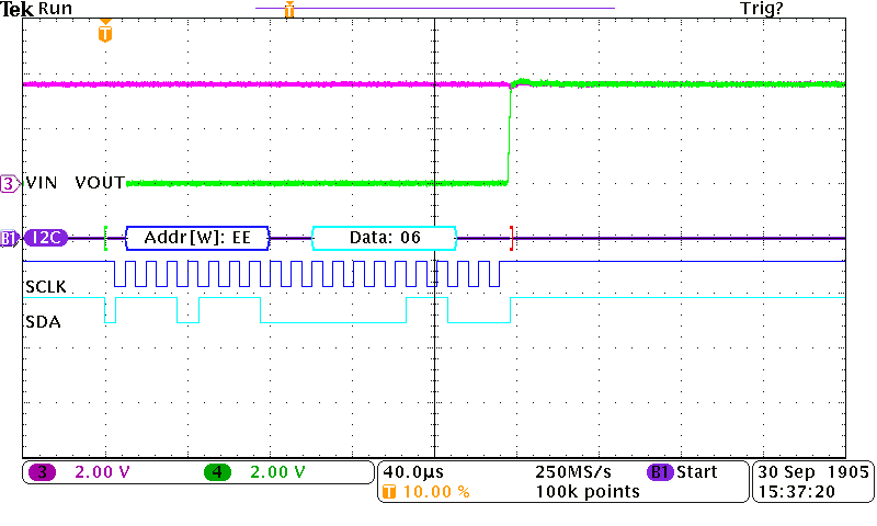
10.1.6 Turn-on/Turn-off of Channels
By default upon power up VBIAS, all the channels of the TPS22994 are controlled via the ONx pins. Using the I2C interface, each channel be controlled via I2C control as well. The channels of the TPS22994 can also be switched on or off by writing to the control register of the device. Each device has a single control register and is located at register address 05h. The register’s composition is as follows:
| Control Register (Address: 05h) |
| BIT | B7 | B6 | B5 | B4 | B3 | B2 | B1 | B0 |
|---|---|---|---|---|---|---|---|---|
| DESCRIPTION | GPIO/I2C CH 4 | GPIO/I2C CH 3 | GPIO/I2C CH 2 | GPIO/I2C CH 1 | ENABLE CH 4 | ENABLE CH 3 | ENABLE CH 2 | ENABLE CH 1 |
| DEFAULT | 0 | 0 | 0 | 0 | 0 | 0 | 0 | 0 |
The lower four bits of the control register dictate if the channels of the device are off (bit set to ‘0’) or on (bit set to ‘1’) during I2C control. The transition from off to on can be made with a single write command to the control register. See Figure 44 for the composition of a single write command.
10.2 Typical Application
10.2.1 Tying Multiple Channels in Parallel
Two or more channels of the device can be tied in parallel for applications that require lower RON and/or more continous current. Tying two channels in parallel will result in half of the RON and two times the IMAX capability. Tying three channels in parallel will result in one-third of the RON and three times the IMAX capability. Tying four channels in parallel will result in one-fourth of the RON and four times the IMAX capability. For the channels that are tied in parallel, it is recommended that the ONx pins be tied together for synchronous control of the channels when in GPIO control. In I2C control, all four channels can be enabaled or disabled synchronously by writing to the control register of the device. Figure 54 shows an application example of tying all four channels in parallel.
 Figure 54. Parallel Channels
10.2.1.1 Design Requirements
Refer to Design Requirements.
10.2.1.2 Detailed Design Procedure
Refer to Detailed Design Procedure.
The only difference between single channel and multiple channels in parallel is the resulting RON and voltage drop from VINx to VOUTx. Thus, the design procedure is identical to Detailed Design Procedure. The VINx to VOUTx voltage drop in the device is determined by the RON of the device and the load current. The RON of the device depends upon the VIN conditions of the device. Refer to the RON specification of the device in the Electrical Characteristics table of this datasheet. Once the RON of the device is determined based upon the VINx conditions, use the following equation to calculate the VINx to VOUTx voltage drop:
Where:
ΔV = voltage drop from VINx to VOUTx
ILOAD = load current
RON = On-resistance of the device for a specific VIN
K = number of channels in parallel (2, 3, or 4)
An appropriate ILOAD must be chosen such that the IMAX specification per channel of the device is not violated.
10.2.1.3 Application Curves
Refer to Application Curves.
10.2.2 Cold Boot Programming of All Registers
Since the TPS22994 has a digital core with volatile memory, upon power cycle of the VBIAS pin, the registers will revert back to their default values (see register map for default values). Therefore, the application must reprogram the configuration registers, control register, and mode registers if non-default values are desired. The TPS22994 contains 17 programmable registers (4 configuration registers, 1 control register, 12 mode registers) in total.
During cold boot when the microcontroller and the I2C bus is not yet up and running, the channels of the TPS22994 can still be enabled via GPIO control. One method to achieve this is to tie the ONx pin to the respective VINx pin for the channels that need to turn on by default during cold boot. With this method, when VINx is applied to the TPS22994, the channel will be enabled as well. Once the I2C bus is active, the channel can be switched over to I2C control to be disabled. See Figure 55 for an example of how the ONx pins can be tied to VINx for default enable during cold boot.
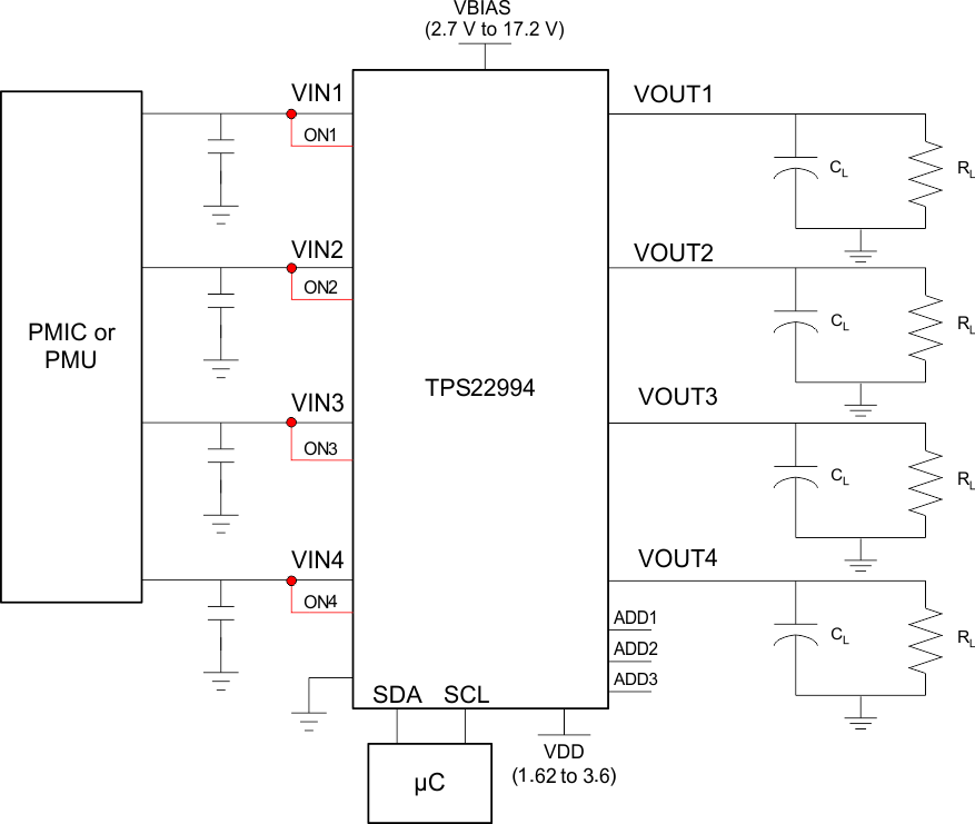 Figure 55. Cold Boot Programming
10.2.2.1 Design Requirements
Refer to Design Requirements.
10.2.2.2 Detailed Design Procedure
Refer to Design Requirements.
10.2.2.3 Application Curves
Refer to Application Curves.
10.2.3 Power Sequencing Without I2C
It is also possible to power sequence the channels of the device during a cold boot when there is no I2C bus present for control. One method to accomplish this it to tie the VOUT of one channel to the ON pin of the next channel in the sequence. For example, if the desired power up sequence is VOUT3, VOUT1, VOUT2, and VOUT4 (in that order), then the device can be configured for GPIO control as shown in Figure 56. The device will power up with default slew rate, ON-delay, and QOD values as specified in the register map.
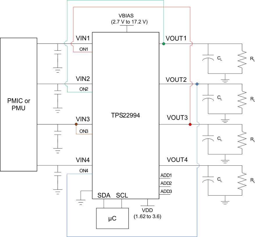 Figure 56. Power Sequencing Without I2C Schematic
10.2.3.1 Design Requirements
10.2.3.1.1 Reading From the Registers
Reading any register from the TPS22994 follows the same standard I2C read protocol as outlined in the I2C Protocol section of this datasheet.
For this design example, use the following as the input parameters:
| DESIGN PARAMETER | EXAMPLE VALUE |
|---|---|
| VINx | 3.3 V |
| Load Current | 1 A |
10.2.3.2 Detailed Design Procedure
To begin the design process, the designer needs to know the following:
- VINx voltage
- Load Current
10.2.3.2.1 VIN to VOUT Voltage Drop
The VINx to VOUTx voltage drop in the device is determined by the RON of the device and the load current. The RON of the device depends upon the VIN conditions of the device. Refer to the RON specification of the device in the Electrical Characteristics table of this datasheet. Once the RON of the device is determined based upon the VINx conditions, use Equation 2 to calculate the VINx to VOUTx voltage drop:
Where:
ΔV = voltage drop from VINx to VOUTx
ILOAD = load current
RON = On-resistance of the device for a specific VIN
An appropriate ILOAD must be chosen such that the IMAX specification of the device is not violated.
10.2.3.2.2 Inrush Current
To determine how much inrush current will be caused by the CL capacitor, use Equation 3:

Where:
IINRUSH = amount of inrush caused by CL
CL = capacitance on VOUTx
dt = rise time in VOUT during the ramp up of VOUTx when the device is enabled
dVOUT = change in VOUT during the ramp up of VOUTx when the device is enabled
An appropriate CL value should be placed on VOUTx such that the IMAX specifications of the device are not violated.
10.2.3.3 Application Curves
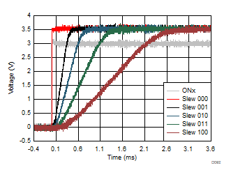
| VBIAS = 7.2V | VINx = 3.6V | VDD = 3.6V |
| RL = 10Ω | TA = 25°C | |
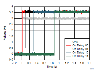
| VBIAS = 7.2V | VINx = 3.6V | VDD = 3.6V |
| RL = 10Ω | TA = 25°C | |
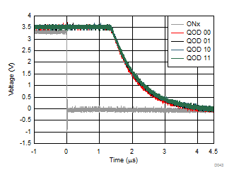
| VBIAS = 7.2V | VINx = 3.6V | VDD = 3.6V |
| RL = 10Ω | TA = 25°C | |
| VBIAS = 7.2V | VINx = 3.6V | VDD = 3.6V |
| RL = 10Ω | TA = 25°C | |
| VBIAS = 7.2V | VINx = 3.6V | VDD = 3.6V |
| RL = 10Ω | TA = 25°C | |
| VBIAS = 7.2V | VINx = 3.6V | VDD = 3.6V |
| RL = Open | TA = 25°C | |
| VBIAS = 7.2V | VINx = 3.6V | VDD = 3.6V |
| RL = 10Ω | TA = 25°C | |
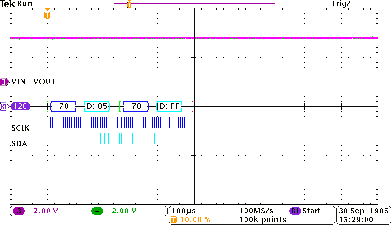
| This example shows the channel of the device being turned on when a I2C "enable" command is written to the register. | ||