ZHCSF80B May   2016  – September 2017 TPS22975

PRODUCTION DATA.  

  1. 特性
  2. 应用
  3. 说明
  4. 修订历史记录
  5. Device Comparison Table
  6. Pin Configuration and Functions
  7. Specifications
    1. 7.1 Absolute Maximum Ratings
    2. 7.2 ESD Ratings
    3. 7.3 Recommended Operating Conditions
    4. 7.4 Thermal Information
    5. 7.5 Electrical Characteristics—VBIAS = 5 V
    6. 7.6 Electrical Characteristics—VBIAS = 2.5 V
    7. 7.7 Switching Characteristics
    8. 7.8 Typical DC Characteristics
    9. 7.9 Typical AC Characteristics
  8. Parameter Measurement Information
  9. Detailed Description
    1. 9.1 Overview
    2. 9.2 Functional Block Diagram
    3. 9.3 Feature Description
      1. 9.3.1 Adjustable Rise Time
      2. 9.3.2 Quick-Output Discharge (QOD) (Optional)
      3. 9.3.3 Thermal Shutdown
    4. 9.4 Device Functional Modes
  10. 10Application and Implementation
    1. 10.1 Application Information
      1. 10.1.1 ON and OFF Control
      2. 10.1.2 Input Capacitor (CIN) (Optional)
      3. 10.1.3 Output Capacitor (CL) (Optional)
    2. 10.2 Typical Application
      1. 10.2.1 Design Requirements
      2. 10.2.2 Detailed Design Procedure
        1. 10.2.2.1 Inrush Current
      3. 10.2.3 Application Curves
  11. 11Power Supply Recommendations
  12. 12Layout
    1. 12.1 Layout Guidelines
    2. 12.2 Layout Example
    3. 12.3 Thermal Considerations
  13. 13器件和文档支持
    1. 13.1 器件支持
      1. 13.1.1 开发支持
    2. 13.2 相关文档
    3. 13.3 接收文档更新通知
    4. 13.4 社区资源
    5. 13.5 商标
    6. 13.6 静电放电警告
    7. 13.7 Glossary
  14. 14机械、封装和可订购信息

封装选项

机械数据 (封装 | 引脚)
散热焊盘机械数据 (封装 | 引脚)
订购信息

Pin Configuration and Functions

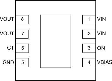
DSG Package
8-Pin (WSON)
Top View
TPS22975 pinout_top_slvsdd0.gif
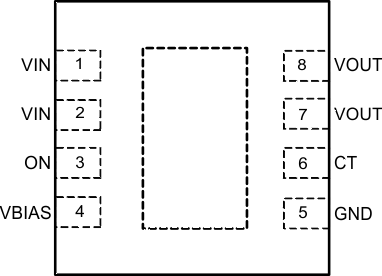
DSG Package
8-Pin (WSON)
Bottom View
TPS22975 pinout_bottom_slvsdd0.gif

Pin Functions

PIN I/O DESCRIPTION
NO. NAME
1 VIN I Switch input. Input bypass capacitor recommended for minimizing VIN dip. Must be connected to Pin 1 and Pin 2. See the Application and Implementation section for more information
2
3 ON I Active high switch control input. Do not leave floating
4 VBIAS I Bias voltage. Power supply to the device. Recommended voltage range for this pin is 2.5 V to 5.7 V. See the Application and Implementation section for more information
5 GND Device ground
6 CT O Switch slew rate control. Can be left floating. See the Adjustable Rise Time section under Feature Description for more information
7 VOUT O Switch output
8
Thermal Pad Thermal pad (exposed center pad) to alleviate thermal stress. Tie to GND. See the Layout Example section for layout guidelines