SLVSDF2A May 2017 – July 2017 TPS22970
PRODUCTION DATA.
- 1 Features
- 2 Applications
- 3 Description
- 4 Revision History
- 5 Pin Configuration and Functions
- 6 Specifications
- 7 Parameter Measurement Information
- 8 Detailed Description
- 9 Application and Implementation
- 10Power Supply Recommendations
- 11Layout
- 12Device and Documentation Support
- 13Mechanical, Packaging, and Orderable Information
6 Specifications
6.1 Absolute Maximum Ratings
over operating free-air temperature range (unless otherwise noted)(1)| MIN | MAX | UNIT | |||
|---|---|---|---|---|---|
| VIN | Input voltage | –0.3 | 4 | V | |
| VOUT | Output voltage | –0.3 | 4 | V | |
| VON | ON voltage | –0.3 | 4 | V | |
| IMAX | Maximum continuous switch current | 4 | A | ||
| IPLS | Maximum pulsed switch current, pulse < 300-µs, 2% duty cycle | 6 | A | ||
| TJ | Maximum junction temperature | Internally Limited | |||
| Tstg | Storage temperature | –65 | 150 | °C | |
(1) Stresses beyond those listed under Absolute Maximum Ratings may cause permanent damage to the device. These are stress ratings only, which do not imply functional operation of the device at these or any other conditions beyond those indicated under Recommended Operating Conditions. Exposure to absolute-maximum-rated conditions for extended periods may affect device reliability.
6.2 ESD Ratings
| VALUE | UNIT | |||
|---|---|---|---|---|
| V(ESD) | Electrostatic discharge | Human-body model (HBM), per ANSI/ESDA/JEDEC JS-001(1) | ±2000 | V |
| Charged-device model (CDM), per JEDEC specification JESD22-C101(2) | ±1000 | |||
(1) JEDEC document JEP155 states that 500-V HBM allows safe manufacturing with a standard ESD control process.
(2) JEDEC document JEP157 states that 250-V CDM allows safe manufacturing with a standard ESD control process.
6.3 Recommended Operating Conditions
over operating free-air temperature range (unless otherwise noted)| MIN | MAX | UNIT | |||
|---|---|---|---|---|---|
| VIN | Input voltage | 0.65 | 3.6 | V | |
| VOUT | Output voltage | VIN | V | ||
| VIH | High-level input voltage, ON | 0.9 | 3.6 | V | |
| VIL | Low-level input voltage, ON | 0 | 0.45 | V | |
| TJ | Operating temperature | –40 | 125 | °C | |
| TA | Operating free-air temperature | –40 | 105 | °C | |
6.4 Thermal Information
| THERMAL METRIC (1) | TPS22970 | UNIT | |
|---|---|---|---|
| YZP (DSBGA) | |||
| 8 PINS | |||
| RθJA | Junction-to-ambient thermal resistance | 130 | °C/W |
| RθJC(top) | Junction-to-case (top) thermal resistance | 54 | °C/W |
| RθJB | Junction-to-board thermal resistance | 51 | °C/W |
| ψJT | Junction-to-top characterization parameter | 1 | °C/W |
| ψJB | Junction-to-board characterization parameter | 50 | °C/W |
(1) For more information about traditional and new thermal metrics, see the Semiconductor and IC Package Thermal Metrics application report.
6.5 Electrical Characteristics
Unless otherwise noted, VIN = 0.65 V to 3.6 V| PARAMETER | TEST CONDITIONS | TA | MIN | TYP | MAX | UNIT | ||
|---|---|---|---|---|---|---|---|---|
| IQ | Quiescent current | VOUT = Open, Switch enabled | VIN > 1.2 V | –40°C to +85°C | 30 | 65 | µA | |
| –40°C to +105°C | 75 | |||||||
| VIN ≤ 1.2 V | –40°C to +85°C | 20 | 50 | |||||
| –40°C to +105°C | 55 | |||||||
| ISD | Shutdown current | VOUT = GND, Switch disabled | VIN > 1.8 V | –40°C to +85°C | 1 | 7.5 | µA | |
| –40°C to +105°C | 18 | |||||||
| VIN ≤ 1.8 V | –40°C to +85°C | 0.9 | 5 | |||||
| –40°C to +105°C | 9.5 | |||||||
| RON | ON-resistance | IOUT = –200 mA | VIN ≥ 1.8 V | 25°C | 4.7 | 8.5 | mΩ | |
| –40°C to +85°C | 9.5 | |||||||
| –40°C to +105°C | 11.5 | |||||||
| VIN = 1.2 V | 25°C | 4.9 | 9.1 | |||||
| –40°C to +85°C | 10.1 | |||||||
| –40°C to +105°C | 12.1 | |||||||
| VIN = 1.05 V | 25°C | 5.1 | 9.4 | |||||
| –40°C to +85°C | 10.4 | |||||||
| –40°C to +105°C | 12.4 | |||||||
| VIN = 0.65 V | 25°C | 6.4 | 11.5 | |||||
| –40°C to +85°C | 12.5 | |||||||
| –40°C to +105°C | 14.5 | |||||||
| RPD | Output pull down resistance(1) | IOUT = 3 mA, Switch disabled | VIN = 3.6 V | –40°C to +105°C | 150 | Ω | ||
| VIN = 0.65 V | –40°C to +105°C | 710 | Ω | |||||
| ION | ON input leakage current | VON = 0 V to 3.6 V | –40°C to +105°C | 0.1 | µA | |||
| TSD | Thermal shutdown | Junction temperature rising | 170 | °C | ||||
| TSD, HYS | Thermal shutdown hysteresis | Junction temperature falling | 30 | °C | ||||
(1) See the Quick Output Discharge (QOD) section.
6.6 Switching Characteristics
over operating free-air temperature range (unless otherwise noted)| PARAMETER | TEST CONDITIONS | MIN | TYP | MAX | UNIT | |
|---|---|---|---|---|---|---|
| VIN = 3.6 V, VON = 3.6 V, TA = 25°C (unless otherwise noted) |
||||||
| tON | Turn-ON time | CL = 0.1 µF, RL = 10 Ω | 1530 | µs | ||
| tOFF | Turn-OFF time | CL = 0.1 µF, RL = 10 Ω | 3.2 | |||
| tR | VOUT Rise time | CL = 0.1 µF, RL = 10 Ω | 985 | |||
| tF | VOUT Fall time | CL = 0.1 µF, RL = 10 Ω | 1.8 | |||
| tD | ON delay time | CL = 0.1 µF, RL = 10 Ω | 550 | |||
| VIN = 1.8 V, VON = 3.6 V, TA = 25°C (unless otherwise noted) |
||||||
| tON | Turn-ON time | CL = 0.1 µF, RL = 10 Ω | 1170 | µs | ||
| tOFF | Turn-OFF time | CL = 0.1 µF, RL = 10 Ω | 4.9 | |||
| tR | VOUT Rise Time | CL = 0.1 µF, RL = 10 Ω | 645 | |||
| tF | VOUT Fall time | CL = 0.1 µF, RL = 10 Ω | 2.2 | |||
| tD | ON delay time | CL = 0.1 µF, RL = 10 Ω | 525 | |||
| VIN = 0.65 V, VON = 3.6 V, TA = 25°C (unless otherwise noted) |
||||||
| tON | Turn-ON time | CL = 0.1 µF, RL = 10 Ω | 815 | µs | ||
| tOFF | Turn-OFF time | CL = 0.1 µF, RL = 10 Ω | 61 | |||
| tR | VOUT Rise time | CL = 0.1 µF, RL = 10 Ω | 320 | |||
| tF | VOUT Fall time | CL = 0.1 µF, RL = 10 Ω | 6.3 | |||
| tD | ON delay time | CL = 0.1 µF, RL = 10 Ω | 495 | |||
6.7 Typical DC Characteristics
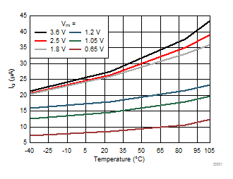
| VON = 3.6 V | VOUT = Open | |
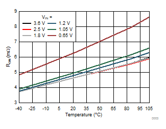
| VON = 3.6 V | IOUT = -200 mA | |
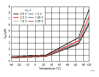
| VON = 0 V | VOUT = GND | |
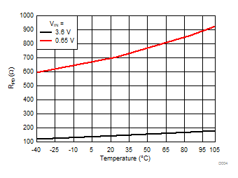
| VON = 0 V | IOUT = 3 mA | |
6.8 Typical AC Characteristics
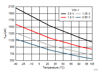 Figure 5. Turn-ON Time vs Temperature
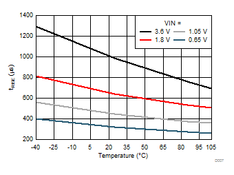 Figure 7. Rise Time vs Temperature
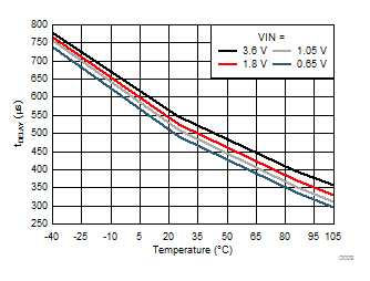
| RL = 10 Ω | CL = 0.1 µF |
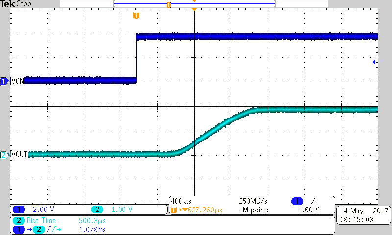
| RL = 10 Ω | TA = 25°C | CL = 0.1 µF |
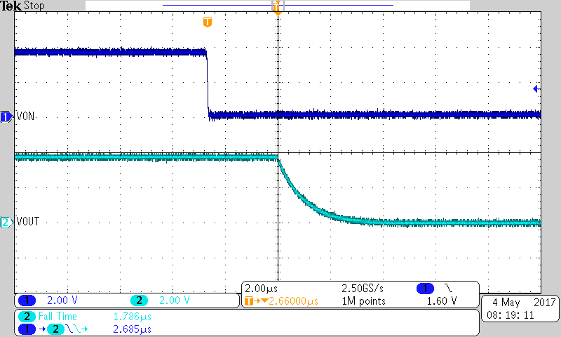
| RL = 10 Ω | TA = 25°C | CL = 0.1 µF |
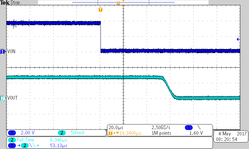
| RL = 10 Ω | TA = 25°C | CL = 0.1 µF |
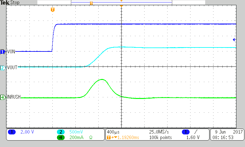
| RL = OPEN | TA = 25°C | CL = 147 µF |
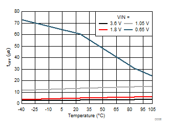 Figure 6. Turn-OFF Time vs Temperature
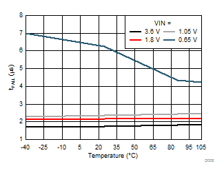
| RL = 10 Ω | CL = 0.1 µF |
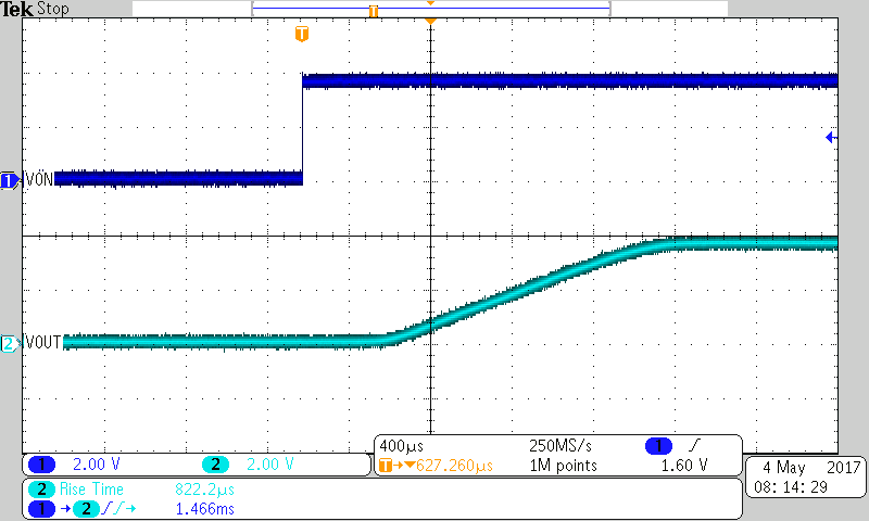
| RL = 10 Ω | TA = 25°C | CL = 0.1 µF |
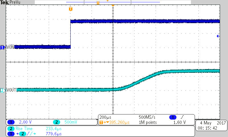
| RL = 10 Ω | TA = 25°C | CL = 0.1 µF |

| RL = 10 Ω | TA = 25°C | CL = 0.1 µF |
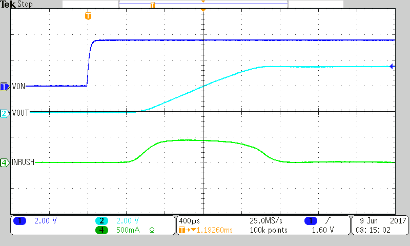
| RL = OPEN | TA = 25°C | CL = 147 µF |