ZHCS613A December   2011  – June 2014 TPS22929D

PRODUCTION DATA.  

  1. 特性
  2. 应用
  3. 说明
  4. 简化电路原理图
  5. 修订历史记录
  6. Pin Configuration and Functions
  7. Specifications
    1. 7.1 Absolute Maximum Ratings
    2. 7.2 Handling Ratings
    3. 7.3 Recommended Operating Conditions
    4. 7.4 Thermal Information
    5. 7.5 Electrical Characteristics
    6. 7.6 Switching Characteristics
    7. 7.7 Typical Characteristics
      1. 7.7.1 Typical AC Characteristics
  8. Parametric Measurement Information
  9. Detailed Description
    1. 9.1 Overview
    2. 9.2 Functional Block Diagram
    3. 9.3 Feature Description
      1. 9.3.1 On/Off Control
      2. 9.3.2 Output Pull-Down
      3. 9.3.3 Under-Voltage Lockout
      4. 9.3.4 Reverse Current Protection
    4. 9.4 Device Functional Modes
  10. 10Application and Implementation
    1. 10.1 Application Information
      1. 10.1.1 VIN to VOUT Voltage Drop
      2. 10.1.2 Input Capacitor
      3. 10.1.3 Output Capacitor
    2. 10.2 Typical Application
      1. 10.2.1 Design Requirements
      2. 10.2.2 Detailed Design Procedure
        1. 10.2.2.1 Managing Inrush Current
      3. 10.2.3 Application Curves
  11. 11Power Supply Recommendations
  12. 12Layout
    1. 12.1 Layout Guidelines
      1. 12.1.1 Thermal Considerations
    2. 12.2 Layout Example
  13. 13器件和文档支持
    1. 13.1 商标
    2. 13.2 静电放电警告
    3. 13.3 术语表
  14. 14机械、封装和可订购信息

封装选项

机械数据 (封装 | 引脚)
散热焊盘机械数据 (封装 | 引脚)
订购信息

Pin Configuration and Functions

SOT23-6 (DBV) PACKAGE
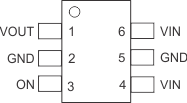
TPS22929D po_lvsb39.gif

Pin Functions

PIN DESCRIPTION
NAME DBV
GND 2, 5 Ground
ON 3 Switch control input, active high. Do not leave floating
VOUT 1 Switch output
VIN 4, 6 Switch input, bypass this input with a ceramic capacitor to ground