ZHCSEX3A February   2016  – March  2016 TPS22918

PRODUCTION DATA.  

  1. 特性
  2. 应用
  3. 说明
  4. 修订历史记录
  5. Pin Configuration and Functions
  6. Specifications
    1. 6.1 Absolute Maximum Ratings
    2. 6.2 ESD Ratings
    3. 6.3 Recommended Operating Conditions
    4. 6.4 Thermal Information
    5. 6.5 Electrical Characteristics
    6. 6.6 Switching Characteristics
    7. 6.7 Typical Characteristics
      1. 6.7.1 DC Characteristics
      2. 6.7.2 AC Characteristics
  7. Parameter Measurement Information
  8. Detailed Description
    1. 8.1 Overview
    2. 8.2 Functional Block Diagram
    3. 8.3 Feature Description
      1. 8.3.1 On and Off Control
      2. 8.3.2 Quick Output Discharge (QOD)
        1. 8.3.2.1 QOD when System Power is Removed
        2. 8.3.2.2 Internal QOD Considerations
      3. 8.3.3 Adjustable Rise Time (CT)
    4. 8.4 Device Functional Modes
  9. Application and Implementation
    1. 9.1 Application Information
    2. 9.2 Typical Application
      1. 9.2.1 Design Requirements
      2. 9.2.2 Detailed Design Procedure
        1. 9.2.2.1 Input Capacitor (CIN)
        2. 9.2.2.2 Output Capacitor (CL) (Optional)
        3. 9.2.2.3 Shutdown Sequencing During Unexpected System Power Loss
        4. 9.2.2.4 VIN to VOUT Voltage Drop
        5. 9.2.2.5 Inrush Current
      3. 9.2.3 Application Curves
  10. 10Power Supply Recommendations
  11. 11Layout
    1. 11.1 Layout Guidelines
    2. 11.2 Layout Example
    3. 11.3 Thermal Considerations
  12. 12器件和文档支持
    1. 12.1 器件支持
      1. 12.1.1 开发支持
    2. 12.2 文档支持
      1. 12.2.1 相关文档 
    3. 12.3 社区资源
    4. 12.4 商标
    5. 12.5 静电放电警告
    6. 12.6 Glossary
  13. 13机械、封装和可订购信息

封装选项

机械数据 (封装 | 引脚)
散热焊盘机械数据 (封装 | 引脚)
订购信息

11 Layout

11.1 Layout Guidelines

VIN and VOUT traces should be as short and wide as possible to accommodate for high current.

The VIN pin should be bypassed to ground with low ESR ceramic bypass capacitors. The typical recommended bypass capacitance is 1-µF ceramic with X5R or X7R dielectric. This capacitor should be placed as close to the device pins as possible.

11.2 Layout Example
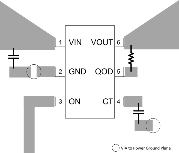
TPS22918 Layout_SLVSD76.gif Figure 32. Recommended Board Layout

11.3 Thermal Considerations

For best performance, all traces should be as short as possible. To be most effective, the input and output capacitors should be placed close to the device to minimize the effects that parasitic trace inductances may have on normal and short-circuit operation. Using wide traces for VIN, VOUT, and GND helps minimize the parasitic electrical effects along with minimizing the case to ambient thermal impedance.

The maximum IC junction temperature should be restricted to 125°C under normal operating conditions. To calculate the maximum allowable dissipation, PD(max) for a given output current and ambient temperature, use Equation 14:

Equation 14. TPS22918 Q5_PDmax2_slvsco0.gif

where

  • PD(MAX) = maximum allowable power dissipation
  • TJ(MAX) = maximum allowable junction temperature (125°C for the TPS22918)
  • TA = ambient temperature of the device
  • θJA = junction to air thermal impedance. Refer to the Thermal Information table. This parameter is highly dependent upon board layout.