ZHCSDR1 April   2015 TPS22860

PRODUCTION DATA.  

  1. 特性
  2. 应用
  3. 说明
  4. 常见应用电路原理图
  5. 修订历史记录
  6. Pin Configuration and Functions
  7. Specifications
    1. 7.1 Absolute Maximum Ratings
    2. 7.2 ESD Ratings
    3. 7.3 Recommended Operating Conditions
    4. 7.4 Thermal Information
    5. 7.5 Electrical Characteristics
    6. 7.6 Switching Characteristics
    7. 7.7 Typical Characteristics
  8. Detailed Description
    1. 8.1 Overview
    2. 8.2 Functional Block Diagram
    3. 8.3 Feature Description
      1. 8.3.1 ON/OFF Control
      2. 8.3.2 Pass Transistor
    4. 8.4 Device Functional Modes
  9. Application and Implementation
    1. 9.1 Application Information
    2. 9.2 Typical Application
      1. 9.2.1 Design Requirements
      2. 9.2.2 Detailed Design Procedure
        1. 9.2.2.1 Inrush Current
        2. 9.2.2.2 ON/OFF Interface
      3. 9.2.3 Application Curves
  10. 10Power Supply Recommendations
  11. 11Layout
    1. 11.1 Layout Guidelines
    2. 11.2 Thermal Reliability
    3. 11.3 Improving Package Thermal Performance
    4. 11.4 Layout Example
  12. 12器件和文档支持
    1. 12.1 商标
    2. 12.2 静电放电警告
    3. 12.3 术语表
  13. 13机械、封装和可订购信息

封装选项

机械数据 (封装 | 引脚)
散热焊盘机械数据 (封装 | 引脚)
订购信息

6 Pin Configuration and Functions

Top View
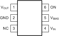
TPS22860 tps22860_pins.gif

Pin Functions

PIN I/O DESCRIPTION
NAME NO.
VOUT 1 O Switch output.
GND 2 Ground
NC 3 No connect
VIN 4 I Switch input. Connect a ceramic capacitor from VIN to GND.
VBIAS 5 I Bias voltage. Power supply to the device.
ON 6 I Active high switch control input. Do not leave floating.