SLVSDQ4 December 2016 TPS2065D
PRODUCTION DATA.
- 1 Features
- 2 Applications
- 3 Description
- 4 Revision History
- 5 Device Comparison Table
- 6 Pin Configuration and Functions
- 7 Specifications
- 8 Detailed Description
- 9 Application and Implementation
- 10Power Supply Recommendations
- 11Layout
- 12Device and Documentation Support
- 13Mechanical, Packaging, and Orderable Information
7 Specifications
7.1 Absolute Maximum Ratings
over operating free-air temperature range (unless otherwise noted)(1)(2)(3)| MIN | MAX | UNIT | ||
|---|---|---|---|---|
| Voltage range on IN, OUT, EN, FLT (3) | –0.3 | 6 | V | |
| Voltage range from IN to OUT | –6 | 6 | V | |
| Maximum junction temperature, TJ | Internally Limited | |||
| Storage temperature, Tstg | –60 | 150 | °C | |
(1) Stresses beyond those listed under Absolute Maximum Ratings may cause permanent damage to the device. These are stress ratings only, which do not imply functional operation of the device at these or any other conditions beyond those indicated under Recommended Operating Conditions. Exposure to absolute-maximum-rated conditions for extended periods may affect device reliability.
(2) Absolute maximum ratings apply over recommended junction temperature range.
(3) Voltages are with respect to GND unless otherwise noted.
(4) VOUT was surged on a pcb with input and output bypassing per Input and Output Capacitance (except input capacitor was 22 µF) with no device failures.
7.2 ESD Ratings
| VALUE | UNIT | |||
|---|---|---|---|---|
| V(ESD) | Electrostatic discharge | Human-body model (HBM), per ANSI/ESDA/JEDEC JS-001(1) | ±2000 | V |
| Charged-device model (CDM), per JEDEC specification JESD22-C101(2) | ±500 | |||
| IEC 61000-4-2 contact discharge (4) | ±8000 | |||
| IEC 61000-4-2 air-gap discharge | ±15000 | |||
(1) JEDEC document JEP155 states that 500-V HBM allows safe manufacturing with a standard ESD control process.
(2) JEDEC document JEP157 states that 250-V CDM allows safe manufacturing with a standard ESD control process.
(3) See Input and Output Capacitance.
7.3 Recommended Operating Conditions
| MIN | NOM | MAX | UNIT | ||
|---|---|---|---|---|---|
| VIN | Input voltage, IN | 4.5 | 5.5 | V | |
| VEN | Input voltage, EN | 0 | 5.5 | V | |
| VIH | High-level input voltage, EN | 2 | V | ||
| VIL | Low-level input voltage, EN | 0.7 | V | ||
| IOUT | Continuous output current, OUT(1) | 1 A | A | ||
| TJ | Operating junction temperature | –40 | 125 | °C | |
| IFLT | Sink current into FLT | 0 | 5 | mA | |
(1) Some package and current rating may request an ambient temperature derating of 85°C.
7.4 Thermal Information
| THERMAL METRIC(1) | TPS2065D | UNIT | |
|---|---|---|---|
| DBV (SOT-23) | |||
| 5 PINS | |||
| RθJA | Junction-to-ambient thermal resistance | 224.9 | °C/W |
| RθJCtop | Junction-to-case (top) thermal resistance | 95.2 | °C/W |
| RθJB | Junction-to-board thermal resistance | 51.4 | °C/W |
| ψJT | Junction-to-top characterization parameter | 6.6 | °C/W |
| ψJB | Junction-to-board characterization parameter | 50.3 | °C/W |
| RθJCbot | Junction-to-case (bottom) thermal resistance | N/A | °C/W |
| RθJACustom | See Power DIssipation and Junction Temperature | 139.3 | °C/W |
(1) For more information about traditional and new thermal metrics, see the Semiconductor and IC Package Thermal Metrics application report.
7.5 Electrical Characteristics: TJ = TA = 25°C(1)
Unless otherwise noted: VIN = 5 V, VEN = VIN, IOUT = 0 A. See Device Comparison Table for the rated current of each part number. Parametrics over a wider operational range are shown in Electrical Characteristics: –40°C ≤ TJ ≤ 125°C.| PARAMETER | TEST CONDITIONS(1) | MIN | TYP | MAX | UNIT | ||
|---|---|---|---|---|---|---|---|
| POWER SWITCH | |||||||
| RDS(on) | Input – output resistance | 1-A rated output, 25°C | DBV | 96 | 110 | mΩ | |
| 1-A rated output, –40°C ≤ (TJ , TA) ≤ 85°C |
DBV | 96 | 130 | mΩ | |||
| CURRENT LIMIT | |||||||
| IOS(3) | Current limit, See Figure 6 | 1-A rated output | 1.3 | 1.55 | 1.8 | A | |
| SUPPLY CURRENT | |||||||
| ISD | Supply current, switch disabled | IOUT = 0 A | 0.01 | 1 | µA | ||
| –40°C ≤ (TJ , TA) ≤ 85°C, VIN = 5.5 V, IOUT = 0 A | 2 | ||||||
| ISE | Supply current, switch enabled | IOUT = 0 A | 60 | 70 | µA | ||
| –40°C ≤ (TJ , TA) ≤ 85°C, VIN = 5.5 V, IOUT = 0 A | 85 | ||||||
| IREV | Reverse leakage current | VOUT = 5 V, VIN = 0 V, measure IVOUT | 0.1 | 1 | µA | ||
| –40°C ≤ (TJ , TA) ≤ 85°C, VOUT = 5 V, VIN = 0 V, measure IVOUT | 5 | ||||||
| OUTPUT DISCHARGE | |||||||
| RPD | Output pulldown resistance(2) | VIN = VOUT = 5 V, disabled | 400 | 470 | 600 | Ω | |
(1) Pulsed testing techniques maintain junction temperature approximately equal to ambient temperature
(2) These parameters are provided for reference only, and do not constitute part of TI's published device specifications for purposes of TI's product warranty.
(3) See Current Limit section for explanation of this parameter.
7.6 Electrical Characteristics: –40°C ≤ TJ ≤ 125°C
Unless otherwise noted:4.5 V ≤ VIN ≤ 5.5 V, VEN = VIN, IOUT = 0 A, typical values are at 5 V and 25°C. See Device Comparison Table for the rated current of each part number.| PARAMETER | TEST CONDITIONS(1) | MIN | TYP | MAX | UNIT | ||
|---|---|---|---|---|---|---|---|
| POWER SWITCH | |||||||
| RDS(ON) | Input – output resistance | 1-A rated output | DBV | 96 | 154 | mΩ | |
| ENABLE INPUT (EN) | |||||||
| Threshold | Input rising | 1 | 1.45 | 2 | V | ||
| Hysteresis | 0.07 | 0.13 | 0.20 | V | |||
| Leakage current | (VEN) = 0 V | –1 | 0 | 1 | µA | ||
| CURRENT LIMIT | |||||||
| IOS(3) | Current limit, See Figure 22 | 1-A rated output | 1.2 | 1.55 | 1.9 | A | |
| tIOS | Short circuit response time(2) | VIN = 5 V (see Figure 6), One-half full load → RSHORT = 50 mΩ, Measure from application to when current falls below 120% of final value |
2 | µs | |||
| SUPPLY CURRENT | |||||||
| ISD | Supply current, switch disabled | IOUT = 0 A | 0.01 | 10 | µA | ||
| ISE | Supply current, switch enabled | IOUT = 0 A | 65 | 90 | µA | ||
| IREV | Reverse leakage current | VOUT = 5.5 V, VIN = 0 V, measure IVOUT | 0.2 | 20 | µA | ||
| UNDERVOLTAGE LOCKOUT | |||||||
| VUVLO | Rising threshold | VIN↑ | 3.5 | 3.75 | 4 | V | |
| Hysteresis(2) | VIN↓ | 0.14 | V | ||||
| FLT | |||||||
| Output low voltage, FLT | IFLT = 1 mA | 0.2 | V | ||||
| Off-state leakage | VFLT = 5.5 V | 1 | µA | ||||
| tFLT | FLT deglitch | FLT assertion or deassertion deglitch | 6 | 9 | 12 | ms | |
| OUTPUT DISCHARGE | |||||||
| RPD | Output pulldown resistance | VIN = 4 V, VOUT = 5 V, disabled | 350 | 560 | 1200 | Ω | |
| VIN = 5 V, VOUT = 5 V, disabled | 300 | 470 | 800 | ||||
| THERMAL SHUTDOWN | |||||||
| Rising threshold (TJ) | In current limit | 135 | °C | ||||
| Not in current limit | 155 | ||||||
| Hysteresis (2) | 20 | ||||||
(1) Pulsed testing techniques maintain junction temperature approximately equal to ambient temperature
(2) These parameters are provided for reference only, and do not constitute part of TI's published device specifications for purposes of TI's product warranty.
(3) See Current Limit for explanation of this parameter.
7.7 Timing Requirements: –40°C ≤ TJ ≤ 125°C
| MIN | NOM | MAX | UNIT | |||
|---|---|---|---|---|---|---|
| tON | Turnon time | VIN = 5 V, CL = 1 µF, RL = 100 Ω, EN ↑ or EN ↓. See Figure 1, Figure 3, and Figure 4 1 A Rated |
1 | 1.4 | 1.8 | ms |
| tOFF | Turnoff time | VIN = 5 V, CL = 1 µF, RL = 100 Ω, EN ↓ or EN ↑. See Figure 1, Figure 3, and Figure 4 1 A Rated |
1.3 | 1.65 | 2 | ms |
| tR | Rise time, output | CL = 1 µF, RL = 100 Ω, VIN = 5 V. See Figure 2
1 A Rated |
0.4 | 0.55 | 0.7 | ms |
| tF | Fall time, output | CL = 1 µF, RL = 100 Ω, VIN = 5 V. See Figure 2
1 A Rated |
0.25 | 0.35 | 0.45 | ms |
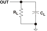 Figure 1. Output Rise and Fall Test Load
 Figure 2. Power-On and Power-Off Timing
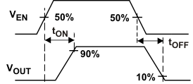 Figure 3. Enable Timing, Active High Enable
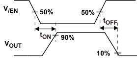 Figure 4. Enable Timing, Active Low Enable
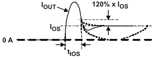 Figure 5. Output Short Circuit Parameters
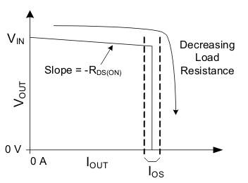 Figure 6. Output Characteristic Showing Current Limit
7.8 Typical Characteristics
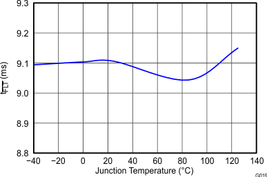
| All Versions, 5 V | ||
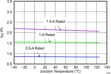
| VIN = 5 V |
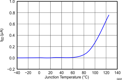
| Input Voltage = 5.5 V |
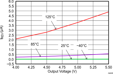
| All Unit Types | VIN = 0 V |
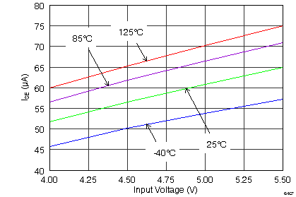
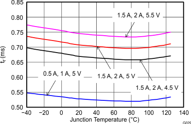
| COUT = 1 µF | RLOAD = 100 Ω |
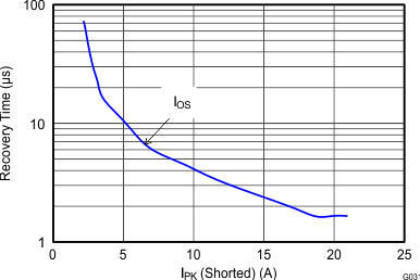
| VIN = 5 V | CIN = 730 µF | IEND = 1.68 A |
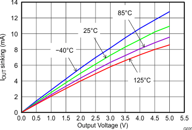
| VIN = 5 V |
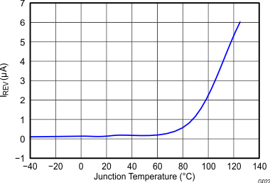
| All Unit Types, 5 V |
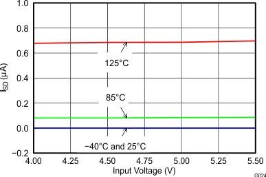
| All Unit Types |
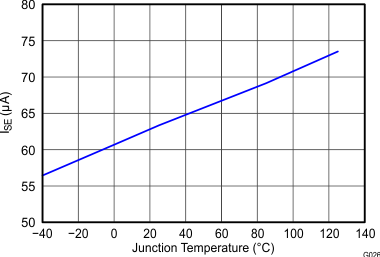
| All Unit Types | VIN = 5.5 V |
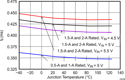
| COUT = 1 µF | RLOAD = 100 Ω |
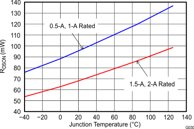
| VIN = 5 V |