SLVSAX6H October 2011 – December 2015 TPS2002C , TPS2003C , TPS2052C , TPS2060C , TPS2062C , TPS2062C-2 , TPS2064C , TPS2064C-2 , TPS2066C , TPS2066C-2
PRODUCTION DATA.
- 1 Features
- 2 Applications
- 3 Description
- 4 Revision History
- 5 Device Comparison Table
- 6 Pin Configuration and Functions
- 7 Specifications
- 8 Parameter Measurement Information
- 9 Detailed Description
- 10Application and Implementation
- 11Power Supply Recommendations
- 12Layout
- 13Device and Documentation Support
- 14Mechanical, Packaging, and Orderable Information
12 Layout
12.1 Layout Guidelines
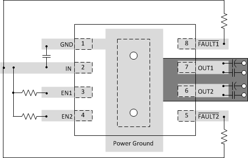
- Place the 100-nF bypass capacitor near the IN and GND pins, and make the connections using a low-inductance trace.
- When large transient currents are expected on the output, TI recommends placing a high-value electrolytic capacitor and a 100-nF bypass capacitor on the output pin.
- The PowerPAD should be directly connected to PCB ground plane using wide and short copper trace.
12.2 Layout Example
 Figure 34. Layout Recommendation
12.3 Power Dissipation and Junction Temperature
It is good design practice to estimate power dissipation and maximum expected junction temperature of the TPS20xxC and TPS20xxC-2 dual. The system designer can control choices of package, proximity to other power dissipating devices, and printed circuit board (PCB) design based on these calculations. These have a direct influence on maximum junction temperature. Other factors such as airflow and maximum ambient temperature are often determined by system considerations.
Addition of extra PCB copper area around these devices is recommended to reduce the thermal impedance and maintain the junction temperature as low as practical.
The following procedure requires iteration because power loss is due to the two internal MOSFETs 2 × I2 × rDS(on), and rDS(on) is a function of the junction temperature. As an initial estimate, use the rDS(on) at 125°C from the typical characteristics, and the preferred package thermal resistance for the preferred board construction from the thermal parameters section.
where
- IOUT = rated OUT pin current (A)
- rDS(on) = Power switch on-resistance at an assumed TJ (Ω)
- TA = Maximum ambient temperature (°C)
- TJ = Maximum junction temperature (°C)
- θJA = Thermal resistance (°C/W)
If the calculated TJ is substantially different from the original assumption, look up a new value of rDS(on) and recalculate.
If the resulting TJ is not less than 125°C, try a PCB construction and/or package with lower θJA.