SLIS093D March 2000 – March 2015 TPIC6C596
PRODUCTION DATA.
- 1 Features
- 2 Applications
- 3 Description
- 4 Revision History
- 5 Pin Configuration and Functions
- 6 Specifications
- 7 Parameter Measurement Information
- 8 Detailed Description
- 9 Application and Implementation
- 10Power Supply Recommendations
- 11Layout
- 12Device and Documentation Support
- 13Mechanical, Packaging, and Orderable Information
封装选项
请参考 PDF 数据表获取器件具体的封装图。
机械数据 (封装 | 引脚)
- PW|16
- N|16
- D|16
散热焊盘机械数据 (封装 | 引脚)
订购信息
9 Application and Implementation
NOTE
Information in the following applications sections is not part of the TI component specification, and TI does not warrant its accuracy or completeness. TI’s customers are responsible for determining suitability of components for their purposes. Customers should validate and test their design implementation to confirm system functionality.
9.1 Application Information
The TPIC6C596 device is a serial-in parallel-out, Power+LogicE 8-bit shift register with low-side switch DMOS outputs rating of a 100 mA per channel. The device is designed to drive resistive and inductive loads and is particularly well-suited as an interface between a microcontroller and LEDs or lamps. The TPIC6C596 device is an enhancement of the TPIC6C595 device, where the shift register serial output (SER OUT) is clocked on the falling edge of the serial clock to provide additional hold-time in applications where several devices are cascaded.
9.1.1 Cascaded Application
The serial output (SEROUT) clocks out of the device on the falling edge of SRCK to provide additional hold time for cascaded applications. Connect the device (SEROUT) pin to the next device (SERIN) for daisy Chain. This provides improved performance for applications where clock signals may be skewed, devices are not located near one another, or the system must tolerate electromagnetic interference.
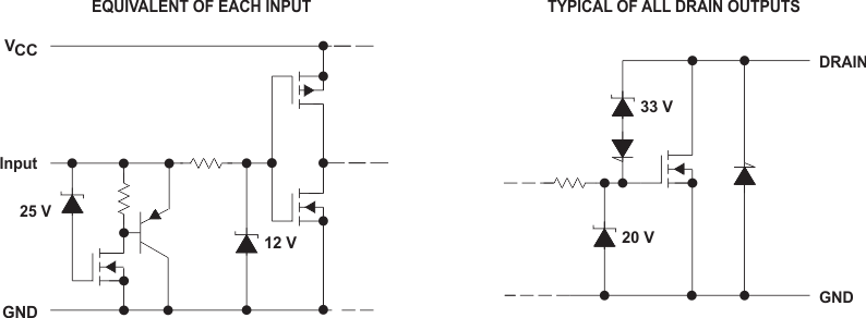
 Figure 13. Schematic of Inputs and Outputs
9.2 Typical Application
The typical application of TPIC6C596 device is an automotive cluster driver. In this example, two TPIC6C596 power shift registers are cascaded and used to turn on LEDs in the cluster panel. In this case, the LED must be updated after all 16 bits of data have been loaded into the serial shift registers. The MCU outputs the data to the serial input (SER IN) while clocking the shift register clock (SRCK). After the 16th clock, a pulse to the register clock (RCK) transfers the data to the storage registers. If output enable (G) is low, then the LEDs are turned on corresponding to the status word with ones being on and zeros off. With this simple scheme, MCU can use the SPI interface to turn on 16 LEDs using only two ICs as illustrated in Figure 14.
 Figure 14. Typical Application Schematic
9.2.1 Design Requirements
Table 1 lists the design parameters for Figure 14.
Table 1. Design Parameters
| DESIGN PARAMTER | EXAMPLE VALUE |
|---|---|
| Vsupply | 9 to16 V |
| V (D1), V (D2), V (D3), V (D4), V (D5), V (D6),V (D7), V (D8) | 2 V |
| V (D9), V (D10),V (D11), V (D12), V (D13), V (D14),V (D15), V (D16) | 3.3 V |
| I (D1), I (D2), I (D3), I (D4), I (D5), I (D6),I (D7), I (D8) | 20 mA when Vbattery is 12 V |
| I (D9), I (D10), I (D11), I (D12), I (D13), I (D14),I (D15), I (D16) | 30 mA when Vbattery is 12 V |
9.2.2 Detailed Design Procedure
To begin the design process, the designer must decide on a few parameters. The designer must know the following:
- Vsupply: LED supply is connected directly to the car battery, which has a voltage range from 9 V to 16 V, or fixed voltage. This application connects to the battery directly.
- V(Dx): LED forward voltage
- I(Dx): LED setting current when battery is 12 V.
9.2.2.1 R1, R2, R3, R4, R5, R6, R7, R8 R1 = R2 = R3 = R4 = R5 = R6 = R7 = R8 =
(Vsupply – V (Dx)) / I (Dx) = (12 V – 2 V) / 0.02 A = 500 Ω
When Vsupply is 9 V, I (D1) = I (D2 ) = I (D3) = I (D4) = I (D5) = I (D6) = I (D7) = I (D8) = (Vsupply – V(Dx) ) / Rx = 14 mA.
When Vsupply is 16 V, I (D9) = I (D10) = I (D11) = I (D12) = I (D13) = I (D14) = I (D15) = I (D16) =(Vsupply – V(Dx)) / Rx= 43.8 mA.
NOTE
If designers can accept the current variation when battery voltage is changing, they can connect the device directly to the battery. If a designer need the less variation of current, they need to use the voltage regulator as supply voltage of LED, or change to constant current LED driver directly
9.2.3 Application Curve
 Figure 15. CH1 is SRCK, CH2 is RCK, CH3 is SER IN and
 CH4 is D1 Current