ZHCSEQ4 July 2015 TPIC2060A
PRODUCTION DATA.
- 1 特性
- 2 应用
- 3 说明
- 4 修订历史记录
- 5 说明 (续)
- 6 Pin Configuration and Functions
- 7 Specifications
-
8 Detailed Description
- 8.1 Overview
- 8.2 Functional Block Diagram
- 8.3 Feature Description
- 8.4 Device Functional Modes
- 8.5 Programming
- 8.6
Register Maps
- 8.6.1 Register State Transition
- 8.6.2 DAC Register (12-Bit Write Only)
- 8.6.3 Control Register (8-Bit Read/Write)
- 8.6.4
Detailed Register Description
- 8.6.4.1 REG01 12-Bit DAC for Tilt (offset = 01h)
- 8.6.4.2 REG02 12-Bit DAC for Focus (offset = 02h)
- 8.6.4.3 REG03 12-Bit DAC for Tracking (offset = 03h)
- 8.6.4.4 REG04 12-Bit DAC for Sled1 (offset = 04h)
- 8.6.4.5 REG05 12-Bit DAC for Sled2 (offset = 05h)
- 8.6.4.6 REG06 12-Bit DAC for Stepping1 (offset = 06h)
- 8.6.4.7 REG07 12-Bit DAC for Stepping2 (offset = 07h)
- 8.6.4.8 REG08 12-Bit DAC for Spindle (offset = 08h)
- 8.6.4.9 REG09 12-Bit DAC for Load (offset = 09h)
- 8.6.4.10 REG70 8-Bit Control Register for DriverEna (offset = 70h)
- 8.6.4.11 REG71 8-Bit Control Register for FuncEna (offset = 71h)
- 8.6.4.12 REG72 8-Bit Control Register for ACTCfg (offset = 72h)
- 8.6.4.13 REG73 8-Bit Control Register for Parm0 (offset = 73h)
- 8.6.4.14 REG74 8-Bit Control Register for SIFCfg (offset = 74h)
- 8.6.4.15 REG75 8-Bit Control Register for Parm1 (offset = 75h)
- 8.6.4.16 REG76 8-Bit Control Register for WriteEna (offset = 76h)
- 8.6.4.17 REG77 8-Bit Control Register for ClrReg (offset = 77h)
- 8.6.4.18 REG78 8-Bit Control Register for ActTemp (offset = 78h)
- 8.6.4.19 REG79 8-Bit Control Register for UVLOMon (offset = 79h)
- 8.6.4.20 REG7A 8-Bit Control Register for TSDMon (offset = 7Ah)
- 8.6.4.21 REG7B 8-Bit Control Register for SCPMon (offset = 7Bh)
- 8.6.4.22 REG7C 8-Bit Control Register for TempMon (offset = 7Ch)
- 8.6.4.23 REG7D 8-Bit Control Register for Status Monitor (offset = 7Dh)
- 8.6.4.24 REG7E 8-Bit Control Register for Version (offset = 7Eh)
- 8.6.4.25 REG7F 8-Bit Control Register for Status (offset = 7Fh)
- 8.6.4.26 REG60 8-Bit Control Register for SPMCfg (offset = 60h)
- 8.6.4.27 REG61 8-Bit Control Register for SPMCfg (offset = 61h)
- 8.6.4.28 REG62 8-Bit Control Register for SPMCfg (offset = 62h)
- 8.6.4.29 REG64 8-Bit Control Register for Protect (offset = 64h)
- 8.6.4.30 REG65 8-Bit Control Register for SPMCfg (offset = 65h)
- 8.6.4.31 REG68 8-Bit Control Register for Protect (offset = 68h)
- 8.6.4.32 REG6B 8-Bit Control Register for DisProt (offset = 6Bh)
- 8.6.4.33 REG6C 8-Bit Control Register for ENDCfg (offset = 6Ch)
- 8.6.4.34 REG6E 8-Bit Control Register for UtilCfg (offset = 6Eh)
- 8.6.4.35 REG6F 8-Bit Control Register for GPOUTSet (offset = 6Fh)
-
9 Application and Implementation
- 9.1
Application Information
- 9.1.1 DAC Type
- 9.1.2 Example of 12-Bit DAC Sampling Rate for FCS/TRK/TLT
- 9.1.3 Digital Input Coding
- 9.1.4 Example Timing of Target Control System
- 9.1.5 Spindle Motor Driver Operating Sequence
- 9.1.6 Auto Short Brake Function
- 9.1.7 Spindle PWM Control
- 9.1.8 Spindle Driver Current Limit Circuit
- 9.1.9 Sled Driver Part
- 9.1.10 Stepping Driver Part
- 9.1.11 Focus/Track/Tilt Driver Part
- 9.1.12 Load Driver Part
- 9.1.13 End Detect Function
- 9.1.14 Load Tray Lock Detect Function
- 9.1.15 Load Tray Push Detect Function
- 9.1.16 Monitor Signal on GPOUT
- 9.1.17 9-V LDO
- 9.2 Typical Application
- 9.1
Application Information
- 10Power Supply Recommendations
- 11Layout
- 12器件和文档支持
- 13机械、封装和可订购信息
11 Layout
11.1 Layout Guidelines
- CV3P3V, CA5V, and C10V requires external capacitor. Because these are reference voltage for device, locate the capacitor as close to device as possible. Keep away from noise source.
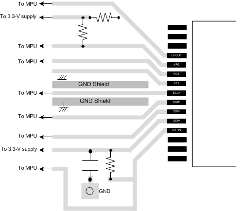
- TI recommends SCLK ground shielding.
- LINFB is feedback pin for LDO. External divided resistors should be located closer to LINFB pin.
11.2 Layout Example

A. GND shield is recommend for SCLK.
Figure 67. Layout Example between TPIC2060A and MPU