ZHCS116G May 2011 – December 2015 TPD4S014
PRODUCTION DATA.
- 1 特性
- 2 应用范围
- 3 说明
- 4 修订历史记录
- 5 Pin Configuration and Functions
- 6 Specifications
-
7 Detailed Description
- 7.1 Overview
- 7.2 Functional Block Diagram
- 7.3
Feature Description
- 7.3.1 Input Voltage Protection at VBUS up to 28 V DC
- 7.3.2 Low RON nFET Switch
- 7.3.3 ESD Performance D+/D-/ID/VBUS Pins
- 7.3.4 Overvoltage and Undervoltage Lockout Features
- 7.3.5 Capacitance TVS ESD Clamp for USB2.0 Hi-Speed Data Rate
- 7.3.6 Start-up Delay
- 7.3.7 OVP Glitch Immunity
- 7.3.8 Integrated Input Enable and Status Output Signal
- 7.3.9 Thermal Shutdown
- 7.4 Device Functional Modes
- 8 Application and Implementation
- 9 Power Supply Recommendations
- 10Layout
- 11器件和文档支持
- 12机械、封装和可订购信息
8 Application and Implementation
NOTE
Information in the following applications sections is not part of the TI component specification, and TI does not warrant its accuracy or completeness. TI’s customers are responsible for determining suitability of components for their purposes. Customers should validate and test their design implementation to confirm system functionality.
8.1 Application Information
The TPD4S014 is a single-chip solution for USB charger port protection. This device offers low capacitance TVS type ESD clamps for the D+, D–, and standard capacitance for the ID pin. On the VBUS pin, this device can handle over voltage protection up to 28 V. The over voltage lockout feature ensures that if there is a fault condition at the VBUS line TPD4S014 is able to isolate the VBUS line and protect the internal circuitry from damage. In order to let the voltage stabilize before closing the switch there is a 17 ms turn on delay after VBUS crosses the UVLO threshold. This function acts as a de-glitch which prevents unnecessary switching if there is any ringing on the line during connection. Due to the body diode of the nFET switch, if there is a short to ground on VBUS the system is expected to limit the current to VBUSOUT.
8.2 Typical Applications
8.2.1 For Non-OTG USB Systems
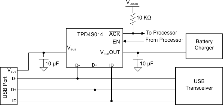 Figure 12. Non-OTG Schematic
8.2.1.1 Design Requirements
Table 2 shows the design parameters.
Table 2. Design Parameters
| DESIGN PARAMETERS | EXAMPLE VALUE |
|---|---|
| Signal range on VBUS | 3.3 V – 5.9 V |
| Signal range on VBUSOUT | 3.9 V – 5.9 V |
| Signal range on D+/D– and ID | 0 V – 5 V |
| Drive EN low (enabled) | 0 V – 0.5 V |
| Drive EN high (disabled) | 1 V – 6 V |
8.2.1.2 Detailed Design Procedure
To begin the design process, some parameters must be decided upon. The designer needs to know the following:
- VBUS voltage range
- Processor logic levels VOH, VOL for EN and VIH, VIL for ACK pins
8.2.2 For OTG USB Systems
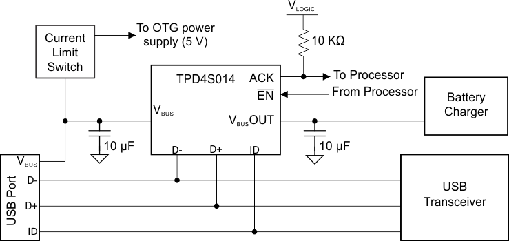 Figure 16. OTG Schematic
8.2.2.1 Design Requirements
Table 3 shows the design parameters.
Table 3. Design Parameters
| DESIGN PARAMETERS | EXAMPLE VALUE |
|---|---|
| Signal range on VBUS | 3.3 V – 5.9 V |
| Signal range on VBUSOUT | 3.9 V – 5.9 V |
| Signal range on D+/D– and ID | 0 V – 5 V |
| Drive EN low (enabled) | 0 V – 0.5 V |
| Drive EN high (disabled) | 1 V – 6 V |
8.2.2.2 Detailed Design Procedure
To begin the design process, some parameters must be decided upon. The designer needs to know the following:
- VBUS voltage range
- Processor logic levels VOH, VOL for EN and VIH, VIL for ACK pins
- OTG power supply output voltage range
8.2.2.3 Application Curves
Refer to Application Curves in the previous section.
