ZHCSB23F March 2013 – September 2017 TPD4E001-Q1
PRODUCTION DATA.
10 Layout
10.1 Layout Guidelines
When placed near the connector, the TPD4E001-Q1 device's ESD solution offers little or no signal distortion during normal operation due to low IO capacitance and ultra-low leakage-current specifications. The TPD4E001-Q1 device ensures that the core circuitry is protected and the system is functioning properly in the event of an ESD strike. For proper operation, observe the following layout and design guidelines:
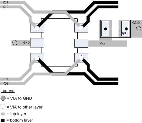
- Place the TPD4E001-Q1 device solution close to the connector. This allows the device to take away the energy associated with ESD strike before it reaches the internal circuitry of the system board.
- Place a 0.1-μF capacitor very close to the VCC pin. This limits any momentary voltage surge at the IO pin during the ESD strike event.
- Ensure that there is enough metallization for the VCC and GND loop. During normal operation, the TPD4E001-Q1 device consumes nA leakage current. But during the ESD event, VCC and GND may see 15 A to 30 A of current, depending on the ESD level. Sufficient current path enables safe discharge of all the energy associated with the ESD strike.
- Leave the unused IO pins floating.
- One can connect the VCC pin in two different ways:
- If the VCC pin connects to the system power supply, the TPD4E001-Q1 works as a transient suppressor for any signal swing above VCC + VF. TI recommends a 0.1-μF capacitor on the device VCC pin for ESD bypass.
- If the VCC pin does not connect to the system power supply, the TPD4E001-Q1 can tolerate higher signal swing in the range up to 10 V. Note that TI still recommends a 0.1-μF capacitor at the VCC pin for ESD bypass.
- The optimum placement is as close to the connector as possible.
- EMI during an ESD event can couple from the trace being struck to other nearby unprotected traces, resulting in early system failures.
- The PCB designer needs to minimize the possibility of EMI coupling by keeping any unprotected traces away from the protected traces which are between the TVS and the connector.
- Route the protected traces as straight as possible.
- Eliminate any sharp corners on the protected traces between the TVS and the connector by using rounded corners with the largest radii possible.
- Electric fields tend to build up on corners, increasing EMI coupling.
10.2 Layout Example
