SLOS992 December 2017 TPA3156D2
PRODUCTION DATA.
- 1 Features
- 2 Applications
- 3 Description
- 4 Revision History
- 5 Pin Configuration and Functions
- 6 Specifications
-
7 Detailed Description
- 7.1 Overview
- 7.2 Functional Block Diagram
- 7.3
Feature Description
- 7.3.1 Gain Setting and Master and Slave
- 7.3.2 Input Impedance
- 7.3.3 Startup and Shutdown Operation
- 7.3.4 PLIMIT Operation
- 7.3.5 GVDD Supply
- 7.3.6 BSPx AND BSNx Capacitors
- 7.3.7 Differential Inputs
- 7.3.8 Device Protection System
- 7.3.9 DC Detect Protection
- 7.3.10 Short-Circuit Protection and Automatic Recovery Feature
- 7.3.11 Thermal Protection
- 7.3.12 Device Modulation Scheme
- 7.3.13 Efficiency: LC Filter Required with the Traditional Class-D Modulation Scheme
- 7.3.14 Ferrite Bead Filter Considerations
- 7.3.15 When to Use an Output Filter for EMI Suppression
- 7.3.16 AM Avoidance EMI Reduction
- 7.4 Device Functional Modes
- 8 Applications and Implementation
- 9 Power Supply Recommendations
- 10Layout
- 11Heat Sink Used on the EVM
- 12Device and Documentation Support
- 13Mechanical, Packaging, and Orderable Information
10 Layout
10.1 Layout Guidelines
The TPA3156D2 can be used with a small, inexpensive ferrite bead output filter for most applications. However, because the class-D switching edges are fast, the layout of the printed circuit board must be planned carefully. The following suggestions will help to meet EMC requirements.
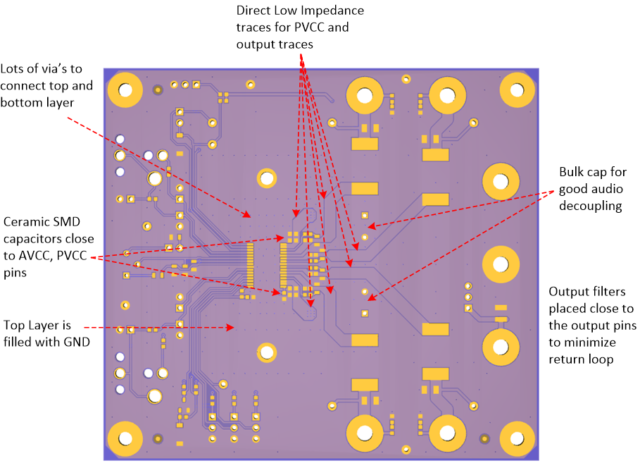
- Decoupling capacitors — The high-frequency decoupling capacitors should be placed as close to the PVCC and AVCC terminals as possible. Large (100 μF or greater) bulk power supply decoupling capacitors should be placed near the TPA3156D2 on the PVCC supplies. Local, high-frequency bypass capacitors should be placed as close to the PVCC pins as possible. These caps can be connected to the IC GND pad directly for an excellent ground connection. Consider adding a small, good quality low ESR ceramic capacitor between 220 pF and 1 nF and a larger mid-frequency cap of value between 100 nF and 1 µF also of good quality to the PVCC connections at each end of the chip.
- Keep the current loop from each of the outputs through the ferrite bead and the small filter cap and back to GND as small and tight as possible. The size of this current loop determines its effectiveness as an antenna.
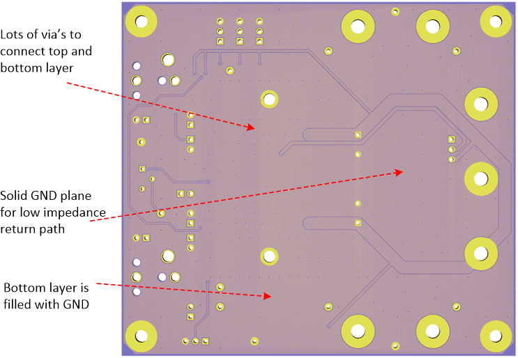
- Grounding — The PVCC decoupling capacitors should connect to GND. All ground should be connected at the IC GND, which should be used as a central ground connection or star ground for the TPA3156D2.
- Output filter — The ferrite EMI filter (see Figure 31) should be placed as close to the output terminals as possible for the best EMI performance. The LC filter should be placed close to the outputs. The capacitors used in both the ferrite and LC filters should be grounded.
For an example layout, see the TPA3156D2 Evaluation Module (TPA3156D2EVM) User Guide (SLOU449). Both the EVM user manual and the thermal pad application reports, SLMA002 and SLMA004, are available on the TI Web site at http://www.ti.com.
10.2 Layout Example
 Figure 37. Layout Example Top
 Figure 38. Layout Example Bottom