SLOS528F July 2009 – April 2017 TPA3110D2
PRODUCTION DATA.
- 1 Features
- 2 Applications
- 3 Description
- 4 Revision History
- 5 Device Comparison Table
- 6 Pin Configuration and F unctions
- 7 Specifications
- 8 Parameter Measurement Information
-
9 Detailed Description
- 9.1 Overview
- 9.2 Functional Block Diagram
- 9.3 Feature Description
- 9.4 Device Functional Modes
- 10Application and Implementation
- 11Power Supply Recommendations
- 12Layout
- 13Device and Documentation Support
- 14Mechanical, Packaging, and Orderable Information
封装选项
机械数据 (封装 | 引脚)
- PWP|28
散热焊盘机械数据 (封装 | 引脚)
- PWP|28
订购信息
6 Pin Configuration and F unctions
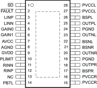
PWP Package
28-Pin HTSSOP With PowerPAD™
Top View

Table 1. Pin Functions
| PIN | TYPE | DESCRIPTION | |
|---|---|---|---|
| NO. | NAME | ||
| 1 | SD | I | Shutdown logic input for audio amp (LOW = outputs Hi-Z, HIGH = outputs enabled). TTL logic levels with compliance to AVCC. |
| 2 | FAULT | O | Open drain output used to display short circuit or dc detect fault status. Voltage compliant to AVCC. Short circuit faults can be set to auto-recovery by connecting FAULT pin to SD pin. Otherwise, both short circuit faults and dc detect faults must be reset by cycling PVCC. |
| 3 | LINP | I | Positive audio input for left channel. Biased at 3 V. |
| 4 | LINN | I | Negative audio input for left channel. Biased at 3 V. |
| 5 | GAIN0 | I | Gain select least significant bit. TTL logic levels with compliance to AVCC. |
| 6 | GAIN1 | I | Gain select most significant bit. TTL logic levels with compliance to AVCC. |
| 7 | AVCC | P | Analog supply |
| 8 | AGND | — | Analog signal ground. Connect to the thermal pad. |
| 9 | GVDD | O | High-side FET gate drive supply. Nominal voltage is 7V. Also should be used as supply for PLIMIT function. |
| 10 | PLIMIT | I | Power limit level adjust. Connect a resistor divider from GVDD to GND to set power limit. Connect directly to GVDD for no power limit. |
| 11 | RINN | I | Negative audio input for right channel. Biased at 3 V. |
| 12 | RINP | I | Positive audio input for right channel. Biased at 3 V. |
| 13 | NC | — | Not connected |
| 14 | PBTL | I | Parallel BTL mode switch |
| 15 | PVCCR | P | Power supply for right channel H-bridge. Right channel and left channel power supply inputs are connect internally. |
| 16 | PVCCR | P | Power supply for right channel H-bridge. Right channel and left channel power supply inputs are connect internally. |
| 17 | BSPR | I | Bootstrap I/O for right channel, positive high-side FET. |
| 18 | OUTPR | O | Class-D H-bridge positive output for right channel. |
| 19 | PGND | — | Power ground for the H-bridges. |
| 20 | OUTNR | O | Class-D H-bridge negative output for right channel. |
| 21 | BSNR | I | Bootstrap I/O for right channel, negative high-side FET. |
| 22 | BSNL | I | Bootstrap I/O for left channel, negative high-side FET. |
| 23 | OUTNL | O | Class-D H-bridge negative output for left channel. |
| 24 | PGND | — | Power ground for the H-bridges. |
| 25 | OUTPL | O | Class-D H-bridge positive output for left channel. |
| 26 | BSPL | I | Bootstrap I/O for left channel, positive high-side FET. |
| 27 | PVCCL | P | Power supply for left channel H-bridge. Right channel and left channel power supply inputs are connect internally. |
| 28 | PVCCL | P | Power supply for left channel H-bridge. Right channel and left channel power supply inputs are connect internally. |