ZHCSNM9B march 2021 – june 2023 TMUX7462F
PRODUCTION DATA
- 1
- 1 特性
- 2 应用
- 3 说明
- 4 Revision History
- 5 Pin Configuration and Functions
-
6 Specifications
- 6.1 Absolute Maximum Ratings
- 6.2 ESD Ratings
- 6.3 Thermal Information
- 6.4 Recommended Operating Conditions
- 6.5 Electrical Characteristics (Global)
- 6.6 ±15 V Dual Supply: Electrical Characteristics
- 6.7 ±20 V Dual Supply: Electrical Characteristics
- 6.8 12 V Single Supply: Electrical Characteristics
- 6.9 36 V Single Supply: Electrical Characteristics
- 6.10 Typical Characteristics
- 7 Parameter Measurement Information
- 8 Detailed Description
- 9 Application and Implementation
- 10Device and Documentation Support
- 11Mechanical, Packaging, and Orderable Information
7.3 Input and Output Leakage Current under Overvoltage Fault
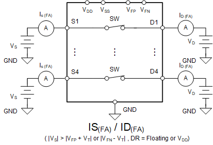
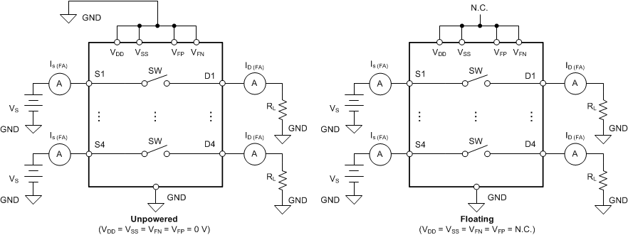
If any of the source pin voltage goes above the fault supplies (VFP or VFN) by one threshold voltage (VT), the TMUX7462F's overvoltage protection feature is triggered to turn off the switch under fault, keeping the fault channel in the high-impedance state. IS(FA) and ID(FA) denotes the input and output leakage current under overvoltage fault conditions, respectively. The supply (or supplies) can either be in normal operating condition (Figure 7-3) or abnormal operating condition (Figure 7-4) when the overvoltage fault occurs. The supply (or supplies) can either be unpowered (VDD= VSS = VFN = VFP = 0 V), floating (VDD= VSS = VFN = VFP = No Connection), or at any level that is below the undervoltage (UV) threshold during abnormal operating conditions.
 Figure 7-3 Measurement Setup for Input and Output Leakage Current Under Overvoltage Fault with Normal Supplies
 Figure 7-4 Measurement Setup for Input and Output Leakage Current Under Overvoltage Fault with Unpowered or Floating Supplies