SPNS225D June 2013 – November 2016 TMS570LS0914
PRODUCTION DATA.
- 1 Device Overview
- 2 Revision History
- 3 Device Comparison
-
4 Terminal Configuration and Functions
- 4.1 Pin Diagrams
- 4.2
Signal Descriptions
- 4.2.1
PGE Package Terminal Functions
- 4.2.1.1 Multibuffered Analog-to-Digital Converters (MibADCs)
- 4.2.1.2 Enhanced High-End Timer (N2HET) Modules
- 4.2.1.3 Enhanced Capture Modules (eCAP)
- 4.2.1.4 Enhanced Quadrature Encoder Pulse Modules (eQEP)
- 4.2.1.5 Enhanced Pulse-Width Modulator Modules (ePWM)
- 4.2.1.6 General-Purpose Input/Output (GIO)
- 4.2.1.7 Controller Area Network Controllers (DCAN)
- 4.2.1.8 Local Interconnect Network Interface Module (LIN)
- 4.2.1.9 Standard Serial Communication Interface (SCI)
- 4.2.1.10 Inter-Integrated Circuit Interface Module (I2C)
- 4.2.1.11 Standard Serial Peripheral Interface (SPI)
- 4.2.1.12 Multibuffered Serial Peripheral Interface Modules (MibSPI)
- 4.2.1.13 System Module Interface
- 4.2.1.14 Clock Inputs and Outputs
- 4.2.1.15 Test and Debug Modules Interface
- 4.2.1.16 Flash Supply and Test Pads
- 4.2.1.17 Supply for Core Logic: 1.2V nominal
- 4.2.1.18 Supply for I/O Cells: 3.3V nominal
- 4.2.1.19 Ground Reference for All Supplies Except VCCAD
- 4.2.2
PZ Package Terminal Functions
- 4.2.2.1 High-End Timer (N2HET) Modules
- 4.2.2.2 Enhanced Capture Modules (eCAP)
- 4.2.2.3 Enhanced Quadrature Encoder Pulse Modules (eQEP)
- 4.2.2.4 Enhanced Pulse-Width Modulator Modules (ePWM)
- 4.2.2.5 General-Purpose Input/Output (GIO)
- 4.2.2.6 Controller Area Network Interface Modules (DCAN1, DCAN2)
- 4.2.2.7 Standard Serial Peripheral Interfaces (SPI2 and SPI4)
- 4.2.2.8 Multibuffered Serial Peripheral Interface (MibSPI1 and MibSPI3)
- 4.2.2.9 Local Interconnect Network Controller (LIN)
- 4.2.2.10 Multibuffered Analog-to-Digital Converter (MibADC)
- 4.2.2.11 System Module Interface
- 4.2.2.12 Clock Inputs and Outputs
- 4.2.2.13 Test and Debug Modules Interface
- 4.2.2.14 Flash Supply and Test Pads
- 4.2.2.15 Supply for Core Logic: 1.2-V Nominal
- 4.2.2.16 Supply for I/O Cells: 3.3-V Nominal
- 4.2.2.17 Ground Reference for All Supplies Except VCCAD
- 4.2.1
PGE Package Terminal Functions
- 4.3 Pin Multiplexing
- 4.4 Buffer Type
-
5 Specifications
- 5.1 Absolute Maximum Ratings
- 5.2 ESD Ratings
- 5.3 Power-On Hours (POH)
- 5.4 Recommended Operating Conditions
- 5.5 Input/Output Electrical Characteristics Over Recommended Operating Conditions
- 5.6 Power Consumption Over Recommended Operating Conditions
- 5.7 Thermal Resistance Characteristics
- 5.8 Timing and Switching Characteristics
-
6 System Information and Electrical Specifications
- 6.1 Device Power Domains
- 6.2 Voltage Monitor Characteristics
- 6.3 Power Sequencing and Power-On Reset
- 6.4 Warm Reset (nRST)
- 6.5 ARM Cortex-R4F CPU Information
- 6.6 Clocks
- 6.7 Clock Monitoring
- 6.8 Glitch Filters
- 6.9 Device Memory Map
- 6.10 Flash Memory
- 6.11 Tightly Coupled RAM Interface Module
- 6.12 Parity Protection for Accesses to Peripheral RAMs
- 6.13 On-Chip SRAM Initialization and Testing
- 6.14 Vectored Interrupt Manager
- 6.15 DMA Controller
- 6.16 Real-Time Interrupt Module
- 6.17 Error Signaling Module
- 6.18 Reset/Abort/Error Sources
- 6.19 Digital Windowed Watchdog
- 6.20 Debug Subsystem
-
7 Peripheral Information and Electrical Specifications
- 7.1 I/O Timings
- 7.2
Enhanced PWM Modules (ePWM)
- 7.2.1 ePWM Clocking and Reset
- 7.2.2 Synchronization of ePWMx Time-Base Counters
- 7.2.3 Synchronizing all ePWM Modules to the N2HET1 Module Time Base
- 7.2.4 Phase-Locking the Time-Base Clocks of Multiple ePWM Modules
- 7.2.5 ePWM Synchronization with External Devices
- 7.2.6 ePWM Trip Zones
- 7.2.7 Triggering of ADC Start of Conversion Using ePWMx SOCA and SOCB Outputs
- 7.2.8 Enhanced Translator-Pulse Width Modulator (ePWMx) Timings
- 7.3 Enhanced Capture Modules (eCAP)
- 7.4 Enhanced Quadrature Encoder (eQEP)
- 7.5 12-Bit Multibuffered Analog-to-Digital Converter (MibADC)
- 7.6 General-Purpose Input/Output
- 7.7 Enhanced High-End Timer (N2HET)
- 7.8 Controller Area Network (DCAN)
- 7.9 Local Interconnect Network Interface (LIN)
- 7.10 Serial Communication Interface (SCI)
- 7.11 Inter-Integrated Circuit (I2C) Module
- 7.12 Multibuffered / Standard Serial Peripheral Interface
- 8 Applications, Implementation, and Layout
- 9 Device and Documentation Support
- 10Mechanical Packaging and Orderable Information
封装选项
请参考 PDF 数据表获取器件具体的封装图。
机械数据 (封装 | 引脚)
- PGE|144
- PZ|100
散热焊盘机械数据 (封装 | 引脚)
订购信息
9 Device and Documentation Support
9.1 Getting Started and Next Steps
To get started using a TMS570 Hercules™ ARM® Cortex®-R Microcontroller (MCU):
- Purchase a TMS570 LaunchPad Development Kit with the LaunchPAD Quickstart Guide included.
- Download the latest version of CCS IDE for Safety MCUs for the specified host platform (that is, Windows, Linux, or MacOS) (free as long as using a LaunchPAD or a Hercules MCU Development Kit [HDK])
- Under Order Now, download the HALCOGEN: HAL Code Generator tool.
- For additional tools and software descriptions, web page links, key docs, and so forth, see Tools and Software.
From the LaunchPAD Quickstart Guide, the user can easily determine the correct Code Composer Studio™ (CCS) Integrated Development Environment (IDE) and Hardware Abstraction Layer Code Generator (HALCoGen™) GUI-based chip configuration tool for any selected Hercules MCU device(s).
The Hercules TMS570 family also has TI BoosterPack™ plug-in modules available that fit on top of a LaunchPad development kit.
9.2 Device and Development-Support Tool Nomenclature
To designate the stages in the product development cycle, TI assigns prefixes to the part numbers of all devices and support tools. Each commercial family member has one of three prefixes: TMX, TMP, or TMS (for example,TMS570LS0914). These prefixes represent evolutionary stages of product development from engineering prototypes (TMX) through fully qualified production devices/tools (TMS).
Device development evolutionary flow:
-
TMX Experimental device that is not necessarily representative of the final device's electrical specifications.
-
TMP Final silicon die that conforms to the device's electrical specifications but has not completed quality and reliability verification.
-
TMS Fully-qualified production device.
TMX and TMP devices are shipped against the following disclaimer:
"Developmental product is intended for internal evaluation purposes."
TMS devices have been characterized fully, and the quality and reliability of the device have been demonstrated fully. TI's standard warranty applies.
Predictions show that prototype devices (TMX or TMP) have a greater failure rate than the standard production devices. Texas Instruments recommends that these devices not be used in any production system because their expected end-use failure rate still is undefined. Only qualified production devices are to be used.
Figure 9-1 shows the numbering and symbol nomenclature for the TMS570LS0914 devices.
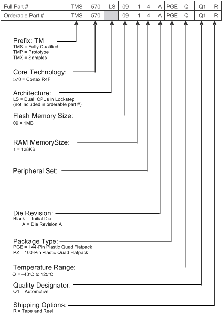 Figure 9-1 TMS570LS0914 Device Numbering Conventions
9.3 Tools and Software
TI offers an extensive line of tools and software for the Hercules™ Safety generation of MCUs including development tools to evaluate the performance of the processors, generate code, develop algorithm implementations, and fully integrate and debug software and hardware modules.
9.3.1 Kits and Evaluation Modules for Hercules TMS570 MCUs
The TMS570 Hercules™ ARM® Cortex®-R Microcontrollers (MCUs) offer a variety of hardware platforms to help speed development. From low-cost LaunchPad™ development kits to full-featured application developer platforms, the Hercules TMS570 MCUs provide a wide range of hardware development tools designed to aid development and get customers to market faster.
Hercules™ TMS570LS12x LaunchPad™ Development Kit
LAUNCHXL2-TMS57012 — The Hercules TMS570LS12x LaunchPad development kit is a low-cost evaluation platform that helps users get started quickly in evaluating and developing with the Hercules microcontroller family, which is specifically designed for ISO 26262 and IEC 61508 functional safety automotive applications. The LaunchPad features onboard emulation for programming and debugging; push-buttons; LEDs and ambient light sensor; and two standard 40-pin BoosterPack expansion connectors. Through the expansion connectors, the LaunchPad development kit can support a wide range of BoosterPack plug-in modules for added functionality (such as displays, wireless sensors, and so forth). LaunchPad development kits come preprogrammed with a demo code that lets the user easily learn the key safety, data acquisition, and control features of the Hercules MCU platform. For additional software downloads and other resources, visit the Hercules LaunchPads wiki.
9.3.2 Development Tools
Development tools includes both hardware and software development tools like integrated development environment (IDE), compilers, and emulators.
Software
Code Composer Studio™ (CCS) Integrated Development Environment (IDE) – Code Composer Studio is an integrated development environment (IDE) that supports TI's Microcontroller and Embedded Processors portfolio. Code Composer Studio comprises a suite of tools used to develop and debug embedded applications. It includes an optimizing C/C++ compiler, source code editor, project build environment, debugger, profiler, and many other features. The intuitive IDE provides a single user interface taking the user through each step of the application development flow. Familiar tools and interfaces allow users to get started faster than ever before. Code Composer Studio combines the advantages of the Eclipse software framework with advanced embedded debug capabilities from TI resulting in a compelling feature-rich development environment for embedded developers.
CCS Uniflash Standalone Flash Tool for TI Microcontrollers (MCUs) [available free of charge] – CCS Uniflash is a standalone tool used to program the on-chip flash memory available on TI MCUs. The CCS Uniflash has a GUI, command line, and scripting interface.
SafeTI™ Compiler Qualification Kit – The SafeTI Compiler Qualification Kit was developed to assist customers in qualifying their use of the TI ARM or C2000 C/C++ Compiler to functional safety standards such as IEC 61508 SIL 3 and ISO 26262 ASIL D.
High-End Timer Integrated Development Environment (HET IDE) – The HET module available on the Hercules MCU devices is a programmable timer coprocessor that enables sophisticated functions for real-time control applications. The HET IDE is a windows-based application that provides an easy way to get started developing and debugging code for the HET module.
Hardware
Below is a list of some emulators that can be used with the Hercules TMS570 MCU devices. For a full list of emulators, click on the Emulators link above.
XDS100v2 – Low-cost, low-performance emulator – integrated on Hercules TMS570 MCU Development Kits. With CCS IDE and IAR support.
XDS200 – The XDS200 is a JTAG emulator for TI embedded processors. Offering a balance of cost and performance, XDS200 emulator fits between the ultra-low cost XDS100 and the high-performance XDS560v2 products.
XDS560v2 – The XDS560™ family of emulators is designed to achieve high download speeds and is ideal for larger applications.
9.3.3 Software
Software includes Real-Time Operating Systems (RTOS), peripheral drivers, libraries, example code, and connectivity.
Hercules MCU software is designed to simplify and speed development of functional safety applications.
Hardware Abstraction Layer Code Generator (HALCoGen) for Hercules MCUs provides a graphical user interface that allows the user to configure peripherals, interrupts, clocks, and many other MCU parameters and can generate driver code which can be easily imported into integrated development environments like CCS IDE, IAR Workbench, etc. The HALCoGen tool also includes several example projects.
SafeTI HALCoGen Compliance Support Package (CSP) assists customers using HALCoGen to comply with functional safety standards by providing example documentation, reports, and unit-test capability.
The SafeTI Hercules Diagnostic Library is a software library of functions and response handlers for various safety features of the Hercules Safety MCUs.
SafeTI Hercules Diagnostic Library CSP assists customers using the SafeTI Diagnostic Library to comply with functional safety standards by providing documentation and reports.
Hercules™ Safety MCU Cortex®-R4 CMSIS DSP Library. The ARM® Cortex® Microcontroller Software Interface Standard (CMSIS) includes over 60 functions covering vector operations, matrix computing, complex arithmetic, filter functions, control functions, PID controller, Fourier transforms, and many other frequently used DSP algorithms. Most algorithms are available in floating-point and various fixed-point formats and are optimized for the Cortex-R series processors.
Hercules™ F021 Flash API provides a software library of functions to program, erase, and verify F021 on-chip flash memory Hercules devices.
The Hercules™ TMS570 MCUs are supported by many different Real-Time Operating Systems (RTOS) and Connectivity/Middleware options from various providers, some of which are safety certified.
9.4 Documentation Support
To receive notification of documentation updates, navigate to the device product folder on ti.com. In the upper right corner, click on Alert me to register and receive a weekly digest of any product information that has changed. For change details, review the revision history included in any revised document.
The following documents describe the processor, related internal peripherals, and other technical collateral with respect to the TMS570LS0914 microcontroller.
Errata
TMS570LS09xx/07xx 16/32-Bit RISC Flash Microcontroller Silicon Errata (Silicon Revision 0) (SPNZ215) describes the known exceptions to the functional specifications for the device.
TMS570LS09xx/07xx 16/32-Bit RISC Flash Microcontroller Silicon Errata (Silicon Revision A) (SPNZ230) describes the known exceptions to the functional specifications for the device.
Technical Reference Manuals
TMS570LS09x/07x 16/32-Bit RISC Flash Microcontroller Technical Reference Manual (SPNU607) details the integration, the environment, the functional description, and the programming models for each peripheral and subsystem in the device.
Applications Reports
Compatibility Considerations: Migrating From TMS570LS31x/21x or TMS570LS12x/11x to TMS570LS0914/0714 Safety Microcontrollers (SPNA204) provides a summary of the differences between the TMS570LS0914/0714 versus the TMS570LS31x/21x and TMS570LS12x/11x series of microcontrollers.
9.5 Community Resources
The following links connect to TI community resources. Linked contents are provided "AS IS" by the respective contributors. They do not constitute TI specifications and do not necessarily reflect TI's views; see TI's Terms of Use.
-
TI E2E™ Online Community The TI engineer-ro-engineer (E2E) community was created to foster collaboration among engineers. At e2e.ti.com, you can ask questions, share knowledge, explore ideas and help solve problems with fellow engineers.
-
TI Embedded Processors Wiki Established to help developers get started with Embedded Processors from Texas Instruments and to foster innovation and growth of general knowledge about the hardware and software surrounding these devices.
-
Hercules™ Safety Microcontrollers Forum TI's Hercules™ Safety Microcontrollers Forum was created under the E2E umbrella to foster collaboration among engineers, ask questions, share knowledge, explore ideas, and help solve problems, specifically relating to the Hercules Safety MCUs (that is, TMS570 and RM families).
-
SafeTI™ Documentation Private E2E Forum A private E2E forum to request access to the safety analysis report; ask questions; share knowledge; and explore ideas to help resolve problems relating to the safety analysis report. This forum is closely monitored by the TI Safety experts. The safety analysis report itself includes detailed device-level Failure Modes, Effects, and Diagnostics Analysis (FMEDA) for ISO 26262 and IEC 61508 functional safety applications. The report also includes tools for estimating module and device-level failure rates (fault insertion tests (FIT) rates).
9.6 Trademarks
BoosterPack, Hercules, LaunchPad, XDS560, E2E are trademarks of Texas Instruments.
CoreSight is a registered trademark of ARM Limited (or its subsidiaries) in the EU and.
ARM, Cortex are registered trademarks of ARM Limited (or its subsidiaries) in the EU and.
All other trademarks are the property of their respective owners.
9.7 Electrostatic Discharge Caution

This integrated circuit can be damaged by ESD. Texas Instruments recommends that all integrated circuits be handled with appropriate precautions. Failure to observe proper handling and installation procedures can cause damage.
ESD damage can range from subtle performance degradation to complete device failure. Precision integrated circuits may be more susceptible to damage because very small parametric changes could cause the device not to meet its published specifications.
9.8 Glossary
-
TI Glossary This glossary lists and explains terms, acronyms, and definitions.
9.9 Device Identification
9.9.1 Device Identification Code Register
The device identification code register at address 0xFFFFFFF0 identifies several aspects of the device including the silicon version. The details of the device identification code register are shown in Table 9-1. The device identification code register value for this device is:
- Rev 0 = 0x8052AD05
- Rev A = 0x8052AD0D
| 31 | 30 | 29 | 28 | 27 | 26 | 25 | 24 | 23 | 22 | 21 | 20 | 19 | 18 | 17 | 16 |
| CP15 | UNIQUE ID | TECH | |||||||||||||
| R-1 | R-00000000101001 | R-0 | |||||||||||||
| 15 | 14 | 13 | 12 | 11 | 10 | 9 | 8 | 7 | 6 | 5 | 4 | 3 | 2 | 1 | 0 |
| TECH | I/O VOLTAGE | PERIPH PARITY | FLASH ECC | RAM ECC | REVISION | 1 | 0 | 1 | |||||||
| R-101 | R-0 | R-1 | R-10 | R-1 | R-00000 | R-1 | R-0 | R-1 | |||||||
| LEGEND: R/W = Read/Write; R = Read only; -n = value after reset |
Table 9-1 Device ID Bit Allocation Register Field Descriptions
| BIT | FIELD | VALUE | DESCRIPTION |
|---|---|---|---|
| 31 | CP15 | Indicates the presence of coprocessor 15 | |
| 1 | CP15 present | ||
| 30-17 | UNIQUE ID | 101001 | Unique device identification number This bitfield holds a unique number for a dedicated device configuration (die). |
| 16-13 | TECH | Process technology on which the device is manufactured. | |
| 0101 | F021 | ||
| 12 | I/O VOLTAGE | I/O voltage of the device. | |
| 0 | I/O are 3.3 V | ||
| 11 | PERIPH PARITY | 1 | Peripheral Parity Parity on peripheral memories |
| 10-9 | FLASH ECC | Flash ECC | |
| 10 | Program memory with ECC | ||
| 8 | RAM ECC | Indicates if RAM ECC is present. | |
| 1 | ECC implemented | ||
| 7-3 | REVISION | Revision of the Device. | |
| 2-0 | 101 | The platform family ID is always 0b101 |
9.9.2 Die Identification Registers
The two die ID registers at addresses 0xFFFFFF7C and 0xFFFFFF80 form a 64-bit dieid with the information as shown in Table 9-2.
Table 9-2 Die-ID Registers
| ITEM | NO. OF BITS | BIT LOCATION |
|---|---|---|
| X Coord. on Wafer | 12 | 0xFFFFFF7C[11:0] |
| Y Coord. on Wafer | 12 | 0xFFFFFF7C[23:12] |
| Wafer # | 8 | 0xFFFFFF7C[31:24] |
| Lot # | 24 | 0xFFFFFF80[23:0] |
| Reserved | 8 | 0xFFFFFF80[31:24] |
9.10 Module Certifications
The following communications modules have received certification of adherence to a standard.
9.10.1 DCAN Certification
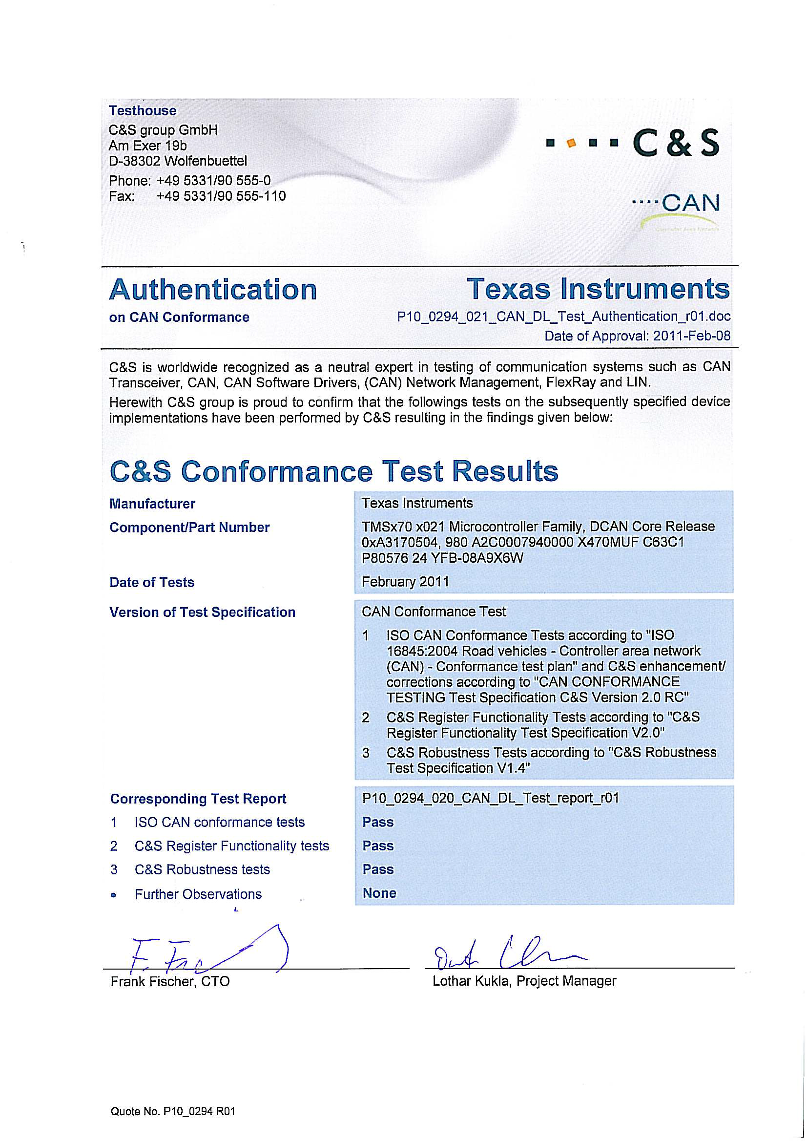 Figure 9-3 DCAN Certification
9.10.2 LIN Certification
9.10.2.1 LIN Master Mode
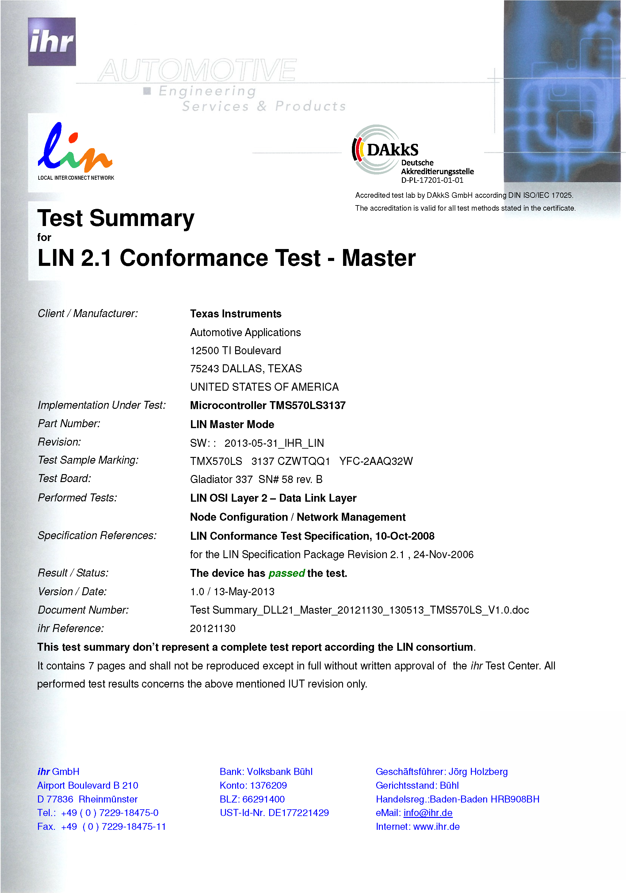 Figure 9-4 LIN Certification - Master Mode
9.10.2.2 LIN Slave Mode - Fixed Baud Rate
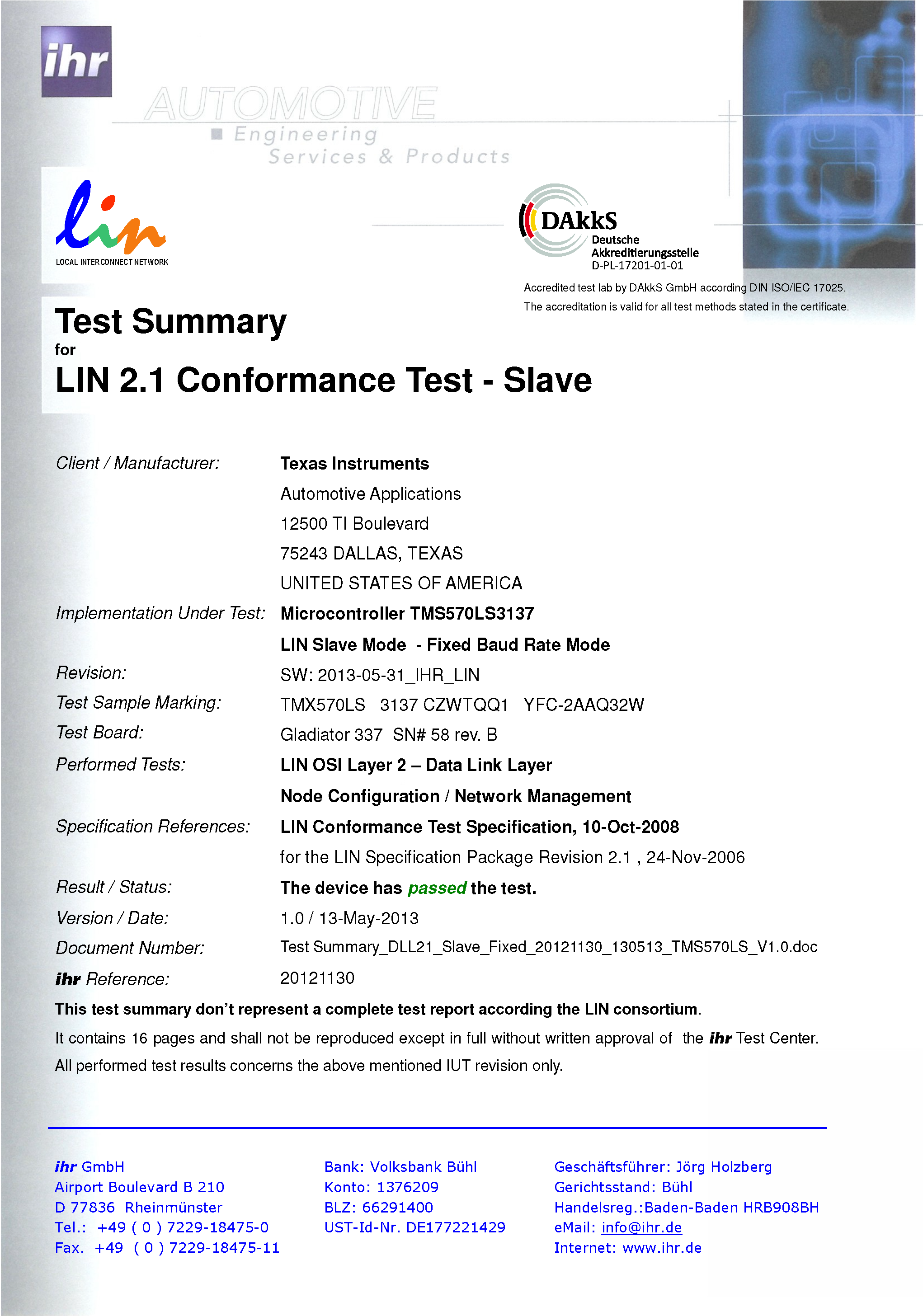 Figure 9-5 LIN Certification - Slave Mode - Fixed Baud Rate
9.10.2.3 LIN Slave Mode - Adaptive Baud Rate
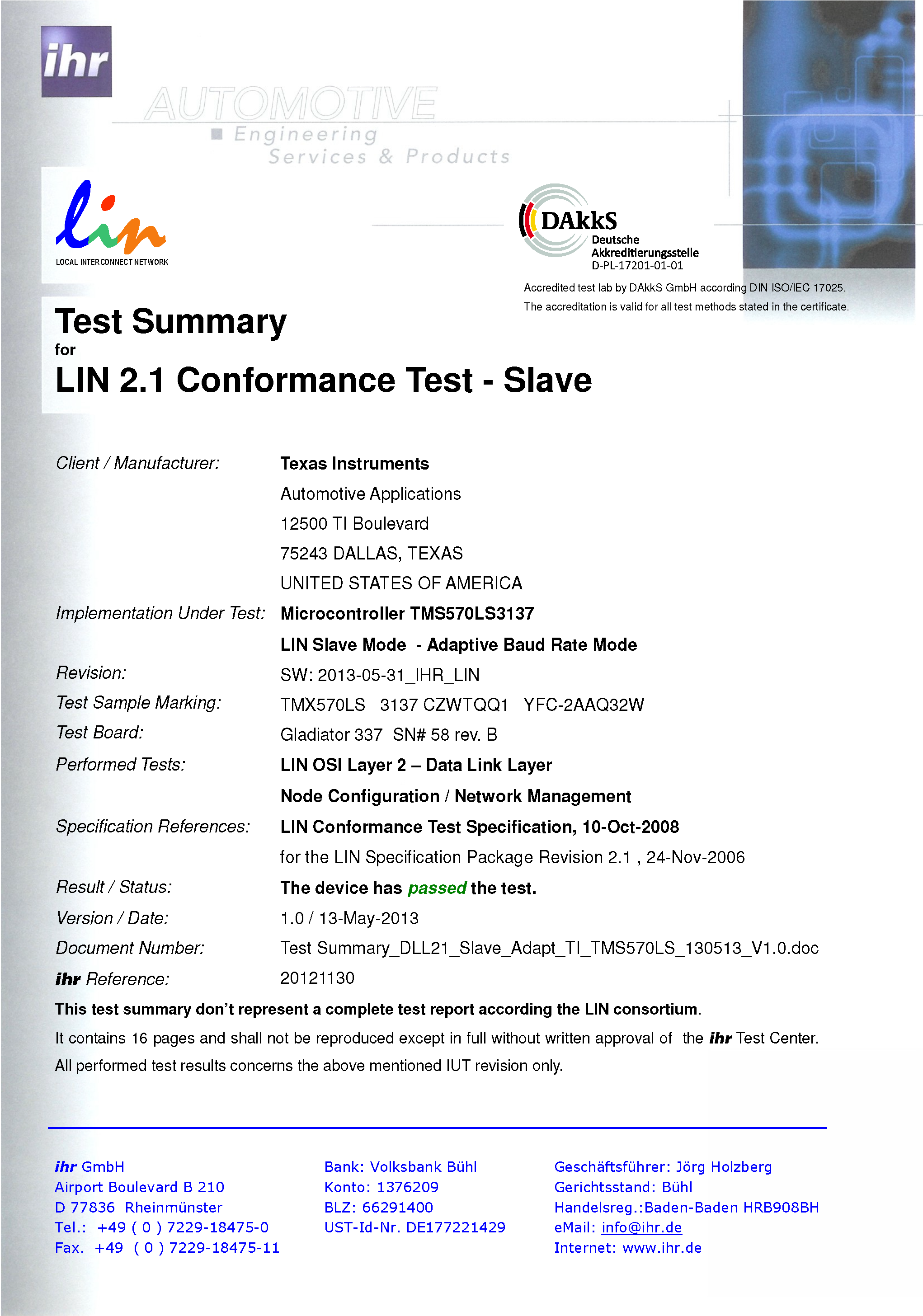 Figure 9-6 LIN Certification - Slave Mode - Adaptive Baud Rate