ZHCS277C August 2011 – April 2014 TMS320C5532 , TMS320C5533 , TMS320C5534 , TMS320C5535
PRODUCTION DATA.
- 1器件概述
- 2修订历史记录
- 3Device Comparison
-
4Terminal Configuration and Functions
- 4.1 Pin Diagram
- 4.2
Signal Descriptions
- 4.2.1 Oscillator and PLL
- 4.2.2 Real-Time Clock (RTC)
- 4.2.3 RESET, Interrupts, and JTAG
- 4.2.4 Inter-Integrated Circuit (I2C)
- 4.2.5 Inter-IC Sound (I2S)
- 4.2.6 Serial Peripheral Interface (SPI)
- 4.2.7 Universal Asynchronous Receiver/Transmitter (UART)
- 4.2.8 Universal Serial Bus (USB) 2.0
- 4.2.9 LCD Bridge
- 4.2.10 Secure Digital (SD)
- 4.2.11 Successive Approximation (SAR) Analog-to-Digital Converter (ADC)
- 4.2.12 General-Purpose Input/Output (GPIO)
- 4.2.13 Regulators and Power Management
- 4.2.14 Reserved and No Connects
- 4.2.15 Supply Voltage
- 4.2.16 Ground
- 4.3 Pin Multiplexing
-
5Specifications
- 5.1 Absolute Maximum Ratings
- 5.2 Recommended Operating Conditions
- 5.3 Electrical Characteristics
- 5.4 Handling Ratings
- 5.5 Thermal Characteristics
- 5.6 Power-On Hours
- 5.7
Timing and Switching Characteristics
- 5.7.1 Parameter Information
- 5.7.2
Power Supplies
- 5.7.2.1 Power Considerations for C5535 and C5534
- 5.7.2.2 Power Considerations for C5533
- 5.7.2.3 Power Considerations for C5532
- 5.7.2.4 Power-Supply Sequencing
- 5.7.2.5 Digital I/O Behavior When Core Power (CVDD) is Down
- 5.7.2.6 Power-Supply Design Considerations
- 5.7.2.7 Power-Supply Decoupling
- 5.7.2.8 LDO Input Decoupling
- 5.7.2.9 LDO Output Decoupling
- 5.7.3
Reset
- 5.7.3.1 Power-On Reset (POR) Circuits
- 5.7.3.2 Pin Behavior at Reset
- 5.7.3.3 Reset Electrical Data and Timing
- 5.7.3.4 Configurations at Reset
- 5.7.3.5
Configurations After Reset
- 5.7.3.5.1 External Bus Selection Register (EBSR)
- 5.7.3.5.2 LDO Control Register [7004h]
- 5.7.3.5.3 USB System Control Registers (USBSCR) [1C32h]
- 5.7.3.5.4 Peripheral Clock Gating Control Registers (PCGCR1 and PCGCR2) [1C02h and 1C03h]
- 5.7.3.5.5 Pullup and Pulldown Inhibit Registers (PDINHIBR1, 2, and 3) [1C17h, 1C18h, and 1C19h]
- 5.7.3.5.6 Output Slew Rate Control Register (OSRCR) [1C16h]
- 5.7.4
Clock Specifications
- 5.7.4.1 Recommended Clock and Control Signal Transition Behavior
- 5.7.4.2 Clock Considerations
- 5.7.4.3 PLLs
- 5.7.4.4 Input and Output Clocks Electrical Data and Timing
- 5.7.4.5 Wake-up Events, Interrupts, and XF
- 5.7.5 Direct Memory Access (DMA) Controller
- 5.7.6 General-Purpose Input/Output
- 5.7.7 General-Purpose Timers
- 5.7.8 Inter-Integrated Circuit (I2C)
- 5.7.9 Inter-IC Sound (I2S)
- 5.7.10 Liquid Crystal Display Controller (LCDC) — C5535 Only
- 5.7.11 Real-Time Clock (RTC)
- 5.7.12 SAR ADC (10-Bit) — C5535 Only
- 5.7.13 Secure Digital (SD)
- 5.7.14 Serial Port Interface (SPI)
- 5.7.15 Universal Asynchronous Receiver/Transmitter (UART)
- 5.7.16 Universal Serial Bus (USB) 2.0 Controller — Does Not Apply to C5532
- 5.7.17 Emulation and Debug
- 5.7.18 IEEE 1149.1 JTAG
-
6Detailed Description
- 6.1 CPU
- 6.2
Memory
- 6.2.1 Internal Memory
- 6.2.2 Memory Map
- 6.2.3
Register Map
- 6.2.3.1 General-Purpose Input/Output Peripheral Register Descriptions
- 6.2.3.2 I2C Peripheral Register Descriptions
- 6.2.3.3 I2S Peripheral Register Descriptions
- 6.2.3.4 LCDC Peripheral Register Descriptions
- 6.2.3.5 RTC Peripheral Register Descriptions
- 6.2.3.6 SAR ADC Peripheral Register Descriptions
- 6.2.3.7 SD Peripheral Register Descriptions
- 6.2.3.8 SPI Peripheral Register Descriptions
- 6.2.3.9 System Registers
- 6.2.3.10 Timers Peripheral Register Descriptions
- 6.2.3.11 UART Peripheral Register Descriptions
- 6.2.3.12 USB2.0 Peripheral Register Descriptions
- 6.3 Identification
- 6.4 Boot Modes
- 7Device and Documentation Support
- 8Mechanical Packaging and Orderable Information
1 器件概述
1.1 特性
- 内核:
- 高性能、低功耗 TMS320C55x 定点数字信号处理器
- 20ns,10ns 指令周期时间
- 50MHz,100MHz 时钟速率
- 每个周期执行一条或两条指令
- 两个乘积累积单元(每秒高达 2 亿次乘积累加运算 [MMACS])
- 两个算术和逻辑单元 (ALU)
- 三个内部数据和操作数读取总线以及两个内部数据和操作数写入总线
- 与 C55x 器件软件兼容
- 提供工业温度器件
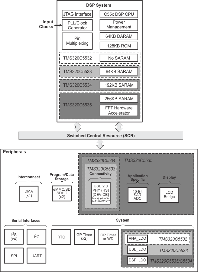
- 320KB 零等待状态片上 RAM,包括:
- 64KB 双访问 RAM (DARAM),8 块 4K x 16 位
- 256KB 单访问 RAM (SARAM),32 块 4K x 16 位
- 128KB 零等待状态片上 ROM
(4 块 16K x 16 位) - 紧密耦合快速傅里叶变换 (FFT) 硬件加速器
- 高性能、低功耗 TMS320C55x 定点数字信号处理器
- 外设:
- 直接存储器存取 (DMA) 控制器
- 四个 DMA,各配有四条通道(共 16 条通道)
- 三个 32 位通用 (GP) 定时器
- 一个可选用为看门狗或 GP
- 两个嵌入式多媒体卡 (eMMC) 和安全数字 (SD) 接口
- 通用异步收发器 (UART)
- 具有四芯片选择的串行端口接口 (SPI)
- 主控和受控内部集成电路(I2C 总线)
- 四个针对数据传输的内部集成电路 (IC) 声音(I2S 总线)
- 带有集成型 2.0 高速物理层 (PHY) 的器件 USB 端口,支持:
- USB 2.0 全速和高速器件
- 具有异步接口的 LCD 桥
- 10 位 4 输入逐次逼近 (SAR) ADC
- IEEE-1149.1 (JTAG)
边界扫描兼容 - 32 个通用 I/O (GPIO) 引脚
(与其它器件功能复用)- 可同时配置最多 20 个 GPIO 引脚
- 直接存储器存取 (DMA) 控制器
- 电源:
- 四个内核隔离的电源域:模拟,RTC,CPU 和外设,以及 USB
- 三个 I/O 隔离电源域:RTC I/O,USB 物理层 (PHY) 和 DVDDIO
- 提供三个集成低压降稳压器 (LDO)(DSP_LDO、ANA_LDO 和 USB_LDO)分别为以下隔离域供电:DSP 内核、模拟和 USB 内核
- 1.05V 内核 (50 MHz),1.8V、2.5V、2.75V 或 3.3V I/O
- 1.3V 内核 (100 MHz),1.8V、2.5V、2.75V 或 3.3V I/O
- 时钟:
- 具有晶振输入、独立时钟域和独立电源的实时时钟 (RTC)
- 低功耗软件可编程锁相环 (PLL) 时钟发生器
- 引导加载程序:
- 片上 ROM 引导加载程序 (RBL),可从 SPI EEPROM、SPI 串行闪存或 I2C EEPROM eMMC、SD、SDHC、UART 和 USB 启动
- 封装:
- 144 端子无铅塑料 BGA(球栅阵列)封装(后缀 ZHH)
1.2 应用
- 无线音频器件(例如:头戴式耳机、麦克风、免提电话)
- 回声消除耳机
- 便携式医疗设备
- 语音应用
- 工业控制
- 指纹识别
- 软件定义的无线电
1.3 说明
这些器件是 TI C5000™ 定点数字信号处理器 (DSP) 产品系列的成员之一,适用于低功耗应用。
定点 DSP 基于 TMS320C55x DSP 系列 CPU 处理器内核。 C55x DSP 架构通过增加的并行性和重视节能来实现高性能和低功耗。 CPU 支持一个内部总线结构,此结构包含一条程序总线,一条 32 位读取总线和两条 16 位数据读取总线,两条数据写入总线和专门用于外设和 DMA 操作的附加总线。 这些总线可实现在一个单周期内执行高达四次 16 位数据读取和两次 16 位数据写入的功能。 此器件还包含四个 DMA 控制器,每个控制器具有 4 条通道,从而在无需 CPU 干预的情况下提供 16 条独立通道环境的数据移动。 每个 DMA 控制器在每周期可执行一个 32 位数据传输,此数据传输与 CPU 的运行并行并且不受 CPU 运行的影响。
C55x CPU 提供两个乘积累积 (MAC) 单元,每个单元在一个单周期内能够进行 17 位乘以 17 位乘法以及 32 位加法。 一个中央 40 位算术和逻辑单元 (ALU) 由一个附加 16 位 ALU 提供支持。 ALU 的使用受指令集控制,从而提供优化并行运行和功耗的能力。 C55x CPU 内的地址单元 (AU) 和数据单元 (DU) 对这些资源进行管理。
C55x CPU 支持一个可变字节宽度指令集以改进代码密度。 指令单元 (IU) 执行从内部或外部存储器中的 32 位程序取指令并且进行针对程序单元 (PU) 的指令排队。 PU 对指令进行解码,将任务指向地址单元和数据单元资源,并管理受到完全保护的管线。 跳转预测功能避免了条件指令执行时的管线冲刷。
TMS320C5535 上的通用输入和输出功能与 10 位 SAR ADC 一起为状态、中断以及用于键盘和媒体接口的位 I/O 提供足够的引脚。 通过以下器件为串行媒体提供支持:两个安全数字 (SD) 外设、四个内部 IC 声音(I2S 总线)模块、一个具有多达四芯片选择的串行端口接口 (SPI)、一个 I2C 主控和受控接口和一个通用异步收发器 (UART) 接口。
其它外设包括:一条仅支持器件模式的高速通用串行总线 (USB2.0)(TMS320C5532 上不提供)、一个实时时钟 (RTC)、三个通用定时器(其中一个可配置为看门狗定时器)和一个模拟锁相环 (APLL) 时钟发生器。
此外,TMS320C5535 还包括紧密耦合 FFT 硬件加速器。 紧密耦合 FFT 硬件加速器支持 8 至 1024 点(2 的幂)实值和复值 FFT。
器件中还包括以下三个集成 LDO,用于为器件的各个部分供电。
ANA_LDO(所有器件)为 DSP PLL (VDDA_PLL)、SAR 和电源管理电路 (VDDA_ANA) 提供 1.3V 电压。
DSP_LDO(TMS320C5535 和 C5534)为 DSP 内核 (CVDD)(一旦检测到工作频率范围,便可由软件实时进行选择)提供 1.3V 或 1.05V 电压。 在最低功耗运行状态下,编程人员可以关断内部 DSP_LDO,切断 DSP 内核 (CVDD) 电源,由外部电源为 RTC (CVDDRTC 和 DVDDRTC) 供电。 可通过 RTC 报警中断或 WAKEUP 引脚重新使能内部 DSP_LDO,然后重新对 DSP 内核加电。 DSP_LDO 复位后,可针对引导加载程序提供 1.3V 工作电压。 对于 50MHz 器件,复位 DSP_LDO 后必须将其设定为 1.05V,使其与内核电压 CVDD 匹配,从而确保正常运行
USB_LDO(TMS320C5535、C5534 和 C5533)为 USB 内核数字电路 (USB_VDD1P3) 和物理层电路 (USB_VDDA1P3) 提供 1.3 V 电压。
这些器件由业界备受赞誉的 eXpressDSP™、 Code Composer Studio™ 集成开发环境 (IDE)、 DSP/BIOS™、德州仪器 (TI) 的算法标准和业界最大的第三方网络提供支持。 Code Composer Studio IDE 提供的代码生成工具包括一个 C 语言编译器和连接器、 RTDX™、XDS100、 XDS510™、 XDS560™ 仿真器件驱动程序和评估模块。 这些器件也受 C55x DSP 库以及芯片支持库的支持,此库特有 50 多个基础软件内核(FIR 滤波器、IIR 滤波器、FFT 和多种数学函数)。
Table 1-1 器件信息
| 部件号 | 封装 | 封装尺寸 |
|---|---|---|
| TMS320C5535AZHH10 | BGA MICROSTAR (144) | 12.0mm x 12.0mm |
| TMS320C5535AZHHA10 | BGA MICROSTAR (144) | 12.0mm x 12.0mm |
| TMS320C5534AZHH10 | BGA MICROSTAR (144) | 12.0mm x 12.0mm |
| TMS320C5534AZHHA10 | BGA MICROSTAR (144) | 12.0mm x 12.0mm |