SBOS371B August 2006 – October 2014 TMP401
PRODUCTION DATA.
- 1 Features
- 2 Applications
- 3 Description
- 4 Revision History
- 5 Pin Configuration and Functions
- 6 Specifications
- 7 Detailed Description
- 8 Application and Implementation
- 9 Power-Supply Recommendations
- 10Layout
- 11Device and Documentation Support
- 12Mechanical, Packaging, and Orderable Information
6 Specifications
6.1 Absolute Maximum Ratings(1)
| MIN | MAX | UNIT | ||
|---|---|---|---|---|
| Power supply, V+ | 7.0 | V | ||
| Input and output voltage(2) | –0.5 | (V+) + (0.5) | V | |
| Input current | 10 | mA | ||
| Operating temperature range | –55 | +125 | °C | |
| Junction Temperature (TJ max) | +150 | °C | ||
(1) Stresses beyond those listed under Absolute Maximum Ratings may cause permanent damage to the device. These are stress ratings only, which do not imply functional operation of the device at these or any other conditions beyond those indicated under Recommended Operating Conditions. Exposure to absolute-maximum-rated conditions for extended periods may affect device reliability.
(2) Input voltage rating applies to all TMP401 input and output pins.
6.2 Handling Ratings
| MIN | MAX | UNIT | |||
|---|---|---|---|---|---|
| Tstg | Storage temperature range | –60 | +130 | °C | |
| V(ESD) | Electrostatic discharge | Human body model (HBM), per ANSI/ESDA/JEDEC JS-001, all pins(1) | –3000 | 3000 | V |
| Charged device model (CDM), per JEDEC specification JESD22-C101, all pins(2) | –1000 | 1000 | |||
(1) JEDEC document JEP155 states that 500-V HBM allows safe manufacturing with a standard ESD control process.
(2) JEDEC document JEP157 states that 250-V CDM allows safe manufacturing with a standard ESD control process.
6.3 Recommended Operating Conditions
| MIN | NOM | MAX | UNIT | ||
|---|---|---|---|---|---|
| V+ | Positive supply (3 V to 5.5 V) | 5 | V | ||
| TA | Ambient temperature | 25 | °C | ||
6.4 Thermal Information
| THERMAL METRIC(1) | TMP401 | UNIT | |
|---|---|---|---|
| DGK (VSSOP) | |||
| 8 PINS | |||
| RθJA | Junction-to-ambient thermal resistance | 78.8 | °C/W |
| RθJC(top) | Junction-to-case (top) thermal resistance | 71.6 | |
| RθJB | Junction-to-board thermal resistance | 68.2 | |
| ψJT | Junction-to-top characterization parameter | 22.0 | |
| ψJB | Junction-to-board characterization parameter | 67.6 | |
| RθJC(bot) | Junction-to-case (bottom) thermal resistance | N/A | |
(1) For more information about traditional and new thermal metrics, see the IC Package Thermal Metrics application report, SPRA953.
6.5 Electrical Characteristics: V+ = 3 V to 5.5 V
At TA = –40°C to +125°C, and V+ = 3 V to 5.5 V, unless otherwise noted.| PARAMETER | TEST CONDITIONS | MIN | TYP | MAX | UNIT | ||
|---|---|---|---|---|---|---|---|
| TEMPERATURE ERROR | |||||||
| TELOCAL | Local temperature sensor | TA = –40°C to +125°C | ±1 | ±3 | °C | ||
| TEREMOTE | Remote temperature sensor(1) | TA = +15°C to +75°C, TREMOTE = –40°C to +150°C,
V+ = 3.3 V |
±1 | °C | |||
| TA = –40°C to +100°C, TREMOTE = –40°C to +150°C, V+ = 3.3 V |
±3 | °C | |||||
| TA = –40°C to +125°C, TREMOTE = –40°C to +150°C | ±5 | °C | |||||
| TELOCAL and TEREMOTE versus supply | V+ = 3 V to 5.5 V | ±0.2 | ±0.5 | °C/V | |||
| TEMPERATURE MEASUREMENT | |||||||
| Conversion time (per channel) | One-shot mode | 115 | ms | ||||
| Resolution | TELOCAL (programmable) | 9 | 12 | Bits | |||
| TEREMOTE | 12 | Bits | |||||
| Remote sensor source currents | High | Series resistance, 3 kΩ max | 120 | µA | |||
| Medium high | 60 | µA | |||||
| Medium low | 12 | µA | |||||
| Low | 6 | µA | |||||
| η | Remote transistor ideality factor | TMP401 optimized ideality factor | 1.008 | ||||
| SMBus INTERFACE | |||||||
| VIH | Logic input high voltage (SCL, SDA) | 2.1 | V | ||||
| VIL | Logic input low voltage (SCL, SDA) | 0.8 | V | ||||
| Hysteresis | 500 | mV | |||||
| SMBus output low sink current | 6 | mA | |||||
| Logic input current | –1 | +1 | µA | ||||
| SMBus input capacitance (SCL, SDA) | 3 | pF | |||||
| SMBus timeout | 30 | 35 | ms | ||||
| DIGITAL OUTPUTS | |||||||
| VOL | Output low voltage | IOUT = 6 mA | 0.15 | 0.4 | V | ||
| IOH | High-level output leakage current | VOUT = V+ | 0.1 | 1 | µA | ||
| ALERT/THERM2 output low sink current | ALERT/THERM2 forced to 0.4 V | 6 | mA | ||||
| THERM output low sink current | THERM forced to 0.4 V | 6 | mA | ||||
| POWER SUPPLY | |||||||
| V+ | Specified voltage range | 3 | 5.5 | V | |||
| IQ | Quiescent current | 0.0625 conversions per second | 29 | 36 | µA | ||
| 8 conversions per second | 390 | 450 | µA | ||||
| Serial bus inactive, shutdown mode | 3 | 10 | µA | ||||
| Serial bus active, fS = 400 kHz, shutdown mode | 90 | µA | |||||
| Serial bus active, fS = 2.5 MHz, shutdown mode | 350 | µA | |||||
| UVLO | Undervoltage lock out | 2.3 | 2.4 | 2.6 | V | ||
| POR | Power-on reset threshold | 1.6 | 2.3 | V | |||
| TEMPERATURE RANGE | |||||||
| Specified range | –40 | +125 | °C | ||||
| Storage range | –60 | +130 | °C | ||||
| θJA | Thermal resistance, VSSOP-8 | 150 | °C/W | ||||
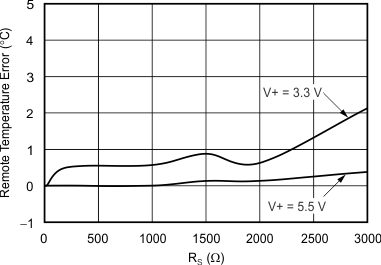
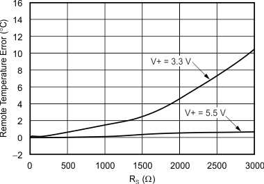
(1) Tested with less than 5-Ω effective series resistance and 100-pF differential input capacitance.
6.6 Timing Requirements
See the Timing Diagrams section for timing diagrams.6.7 Typical Characteristics
At TA = +25°C and V+ = 5.0 V, unless otherwise noted.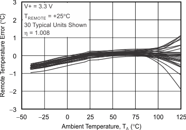


Power-Supply Noise Frequency

SCL Clock Frequency

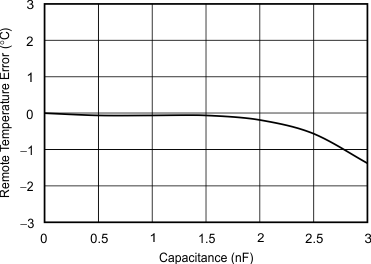
Differential Capacitance

