ZHCSEE7 November   2015 TMP175-Q1 , TMP75-Q1

PRODUCTION DATA.  

  1. 特性
  2. 应用
  3. 说明
  4. 修订历史记录
  5. Pin Configuration and Functions
  6. Specifications
    1. 6.1 Absolute Maximum Ratings
    2. 6.2 ESD Ratings
    3. 6.3 Recommended Operating Conditions
    4. 6.4 Thermal Information
    5. 6.5 Electrical Characteristics
    6. 6.6 Timing Requirements
    7. 6.7 Typical Characteristics
  7. Detailed Description
    1. 7.1 Overview
    2. 7.2 Functional Block Diagram
    3. 7.3 Feature Description
      1. 7.3.1 Digital Temperature Output
      2. 7.3.2 Serial Interface
        1. 7.3.2.1 Bus Overview
        2. 7.3.2.2 Serial Bus Address
        3. 7.3.2.3 Writing and Reading to the TMP175-Q1 and TMP75-Q1
        4. 7.3.2.4 Slave Mode Operations
          1. 7.3.2.4.1 Slave Receiver Mode
          2. 7.3.2.4.2 Slave Transmitter Mode
        5. 7.3.2.5 SMBus Alert Function
        6. 7.3.2.6 General Call
        7. 7.3.2.7 High-Speed Mode
        8. 7.3.2.8 Time-out Function
      3. 7.3.3 Timing Diagrams
        1. 7.3.3.1 Two-Wire Timing Diagrams
    4. 7.4 Device Functional Modes
      1. 7.4.1 Shutdown Mode (SD)
      2. 7.4.2 One-Shot (OS)
      3. 7.4.3 Thermostat Mode (TM)
        1. 7.4.3.1 Comparator Mode (TM = 0)
        2. 7.4.3.2 Interrupt Mode (TM = 1)
    5. 7.5 Programming
      1. 7.5.1 Pointer Register
      2. 7.5.2 Temperature Register
      3. 7.5.3 Configuration Register
        1. 7.5.3.1 Polarity (POL)
        2. 7.5.3.2 Fault Queue (F1/F0)
        3. 7.5.3.3 Converter Resolution (R1/R0)
      4. 7.5.4 High- and Low-Limit Registers
  8. Application and Implementation
    1. 8.1 Application Information
    2. 8.2 Typical Application
      1. 8.2.1 Design Requirements
      2. 8.2.2 Detailed Design Procedure
      3. 8.2.3 Application Curve
  9. Power Supply Recommendations
  10. 10Layout
    1. 10.1 Layout Guidelines
    2. 10.2 Layout Example
  11. 11器件和文档支持
    1. 11.1 相关链接
    2. 11.2 社区资源
    3. 11.3 商标
    4. 11.4 静电放电警告
    5. 11.5 Glossary
  12. 12机械、封装和可订购信息

封装选项

机械数据 (封装 | 引脚)
散热焊盘机械数据 (封装 | 引脚)
订购信息

10 Layout

10.1 Layout Guidelines

Place the power-supply bypass capacitor as close as possible to the supply and ground pins. The recommended value of this bypass capacitor is 0.01 μF. Additional decoupling capacitance can be added to compensate for noisy or high-impedance power supplies. Pull up the open-drain output pins SDA, SCL, and ALERT through 5-kΩ pullup resistors.

10.2 Layout Example
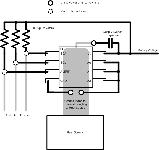
TMP175-Q1 TMP75-Q1 ai_recommended_layout_sbos706.gif Figure 15. Layout Example