ZHCSD13C October   2014  – July 2019 TLV733P

PRODUCTION DATA.  

  1. 特性
  2. 应用
  3. 说明
    1.     Device Images
      1.      典型应用电路
      2.      压降电压与输出电流间的关系
  4. 修订历史记录
  5. Pin Configuration and Functions
    1.     Pin Functions
  6. Specifications
    1. 6.1 Absolute Maximum Ratings
    2. 6.2 ESD Ratings
    3. 6.3 Recommended Operating Conditions
    4. 6.4 Thermal Information
    5. 6.5 Electrical Characteristics
    6. 6.6 Typical Characteristics
  7. Detailed Description
    1. 7.1 Overview
    2. 7.2 Functional Block Diagram
    3. 7.3 Feature Description
      1. 7.3.1 Undervoltage Lockout (UVLO)
      2. 7.3.2 Shutdown and Output Enable
      3. 7.3.3 Internal Foldback Current Limit
      4. 7.3.4 Thermal Shutdown
    4. 7.4 Device Functional Modes
      1. 7.4.1 Normal Operation
      2. 7.4.2 Dropout Operation
      3. 7.4.3 Disabled
  8. Application and Implementation
    1. 8.1 Application Information
      1. 8.1.1 Input and Output Capacitor Selection
      2. 8.1.2 Dropout Voltage
      3. 8.1.3 Power Dissipation
    2. 8.2 Typical Applications
      1. 8.2.1 DC-DC Converter Post Regulation
        1. 8.2.1.1 Design Requirements
        2. 8.2.1.2 Design Considerations
        3. 8.2.1.3 Application Curve
      2. 8.2.2 Capacitor-Free Operation from Battery Input Supply
        1. 8.2.2.1 Design Requirements
        2. 8.2.2.2 Design Considerations
        3. 8.2.2.3 Application Curve
  9. Power Supply Recommendations
  10. 10Layout
    1. 10.1 Layout Guidelines
    2. 10.2 Layout Examples
  11. 11器件和文档支持
    1. 11.1 器件支持
      1. 11.1.1 开发支持
        1. 11.1.1.1 评估模块
      2. 11.1.2 器件命名规则
    2. 11.2 文档支持
      1. 11.2.1 相关文档 
    3. 11.3 接收文档更新通知
    4. 11.4 社区资源
    5. 11.5 商标
    6. 11.6 静电放电警告
    7. 11.7 Glossary
  12. 12机械、封装和可订购信息

封装选项

请参考 PDF 数据表获取器件具体的封装图。

机械数据 (封装 | 引脚)
  • DBV|5
  • DQN|4
散热焊盘机械数据 (封装 | 引脚)
订购信息

Power Dissipation

The ability to remove heat from the die is different for each package type, presenting different considerations in the printed circuit board (PCB) layout. The PCB area around the device that is free of other components moves the heat from the device to ambient air. Performance data for JEDEC high-K boards are given in the Thermal Information table. Using heavier copper increases the effectiveness in removing heat from the device. The addition of plated through-holes to heat-dissipating layers also improves heatsink effectiveness.

Power dissipation (PD) depends on input voltage and load conditions. PD is equal to the product of the output current and voltage drop across the output pass element, as shown in Equation 2.

Equation 2. PD = (VIN – VOUT) × IOUT

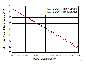
Figure 34 shows the maximum ambient temperature versus the power dissipation of the TLV733 in the DQN and DBV packages. This figure assumes the device is soldered on JEDEC standard high-K layout with no airflow over the board. Actual board thermal impedances vary widely. If the application requires high power dissipation, having a thorough understanding of the board temperature and thermal impedances is helpful to make sure the TLV733 does not operate continuously above a junction temperature of 125°C.
TLV733P D028_sbvs235.gif
TLV733, high-K layout
Figure 34. Maximum Ambient Temperature vs Device Power Dissipation