ZHCSFR4C DECEMBER   2016  – October 2017 TLV62569

UNLESS OTHERWISE NOTED, this document contains PRODUCTION DATA.  

  1. 特性
  2. 应用
  3. 说明
    1.     Device Images
      1.      简化电路原理图
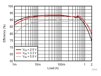
      2. 5V 输入电压下的效率
  4. 修订历史记录
  5. Pin Configuration and Functions
    1.     Pin Functions
  6. Specifications
    1. 6.1 Absolute Maximum Ratings
    2. 6.2 ESD Ratings
    3. 6.3 Recommended Operating Conditions
    4. 6.4 Thermal Information
    5. 6.5 Electrical Characteristics
    6. 6.6 Typical Characteristics
  7. Detailed Description
    1. 7.1 Overview
    2. 7.2 Functional Block Diagrams
    3. 7.3 Feature Description
      1. 7.3.1 Power Save Mode
      2. 7.3.2 100% Duty Cycle Low Dropout Operation
      3. 7.3.3 Soft Startup
      4. 7.3.4 Switch Current Limit
      5. 7.3.5 Under Voltage Lockout
      6. 7.3.6 Thermal Shutdown
    4. 7.4 Device Functional Modes
      1. 7.4.1 Enabling/Disabling the Device
      2. 7.4.2 Power Good
  8. Application and Implementation
    1. 8.1 Application Information
    2. 8.2 Typical Application
      1. 8.2.1 Design Requirements
      2. 8.2.2 Detailed Design Procedure
        1. 8.2.2.1 Custom Design With WEBENCH® Tools
        2. 8.2.2.2 Setting the Output Voltage
        3. 8.2.2.3 Output Filter Design
        4. 8.2.2.4 Inductor Selection
        5. 8.2.2.5 Input and Output Capacitor Selection
      3. 8.2.3 Application Performance Curves
  9. Power Supply Recommendations
  10. 10Layout
    1. 10.1 Layout Guidelines
    2. 10.2 Layout Example
    3. 10.3 Thermal Considerations
  11. 11器件和文档支持
    1. 11.1 器件支持
      1. 11.1.1 Third-Party Products Disclaimer
      2. 11.1.2 开发支持
        1. 11.1.2.1 使用 WEBENCH® 工具创建定制设计
    2. 11.2 文档支持
      1. 11.2.1 相关文档
    3. 11.3 接收文档更新通知
    4. 11.4 社区资源
    5. 11.5 商标
    6. 11.6 静电放电警告
    7. 11.7 Glossary
  12. 12机械、封装和可订购信息

封装选项

机械数据 (封装 | 引脚)
散热焊盘机械数据 (封装 | 引脚)
订购信息

Application Performance Curves

VIN = 5 V, VOUT = 1.8 V, L = 2.2 μH, TA = 25 °C, unless otherwise noted.
TLV62569 TLV62569P D004_SLVSDG1_TLV62569.gif
Figure 6. 1.2-V Output Efficiency
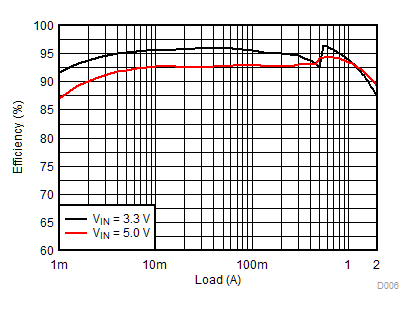
TLV62569 TLV62569P D006_SLVSDG1_TLV62569.gif
Figure 8. 2.5-V Output Efficiency
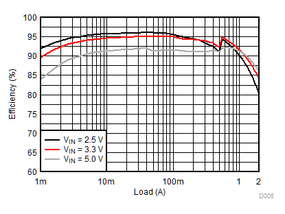
TLV62569 TLV62569P D005_SLVSDG1_TLV62569.gif
Figure 7. 1.8-V Output Efficiency
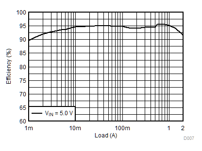
TLV62569 TLV62569P D007_SLVSDG1_TLV62569.gif
Figure 9. 3.3-V Output Efficiency
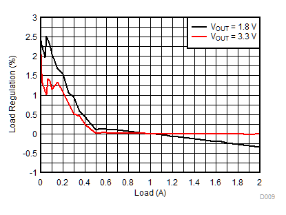
TLV62569 TLV62569P D009_SLVSDG1_TLV62569.gif
VIN = 5 V
Figure 10. Load Regulation
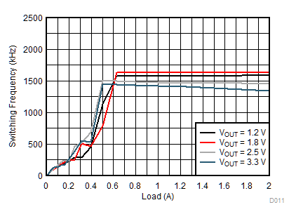
TLV62569 TLV62569P D011_SLVSDG1_TLV62569.gif
VIN = 5 V
Figure 12. Switching Frequency vs Load
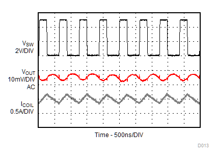
TLV62569 TLV62569P D013_SLVSDG1_TLV62569.gif
IOUT = 1 A
Figure 14. PWM Operation
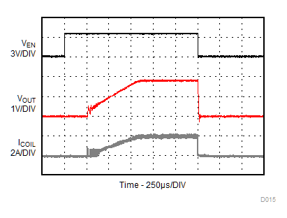
TLV62569 TLV62569P D015_SLVSDG1_TLV62569.gif
IOUT = 2 A
Figure 16. Startup and Shutdown with Load
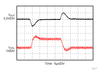
TLV62569 TLV62569P D017_SLVSDG1_TLV62569.gif
Load Step 0.8 A to 2 A, 1A/μs slew rate
Figure 18. Load Transient
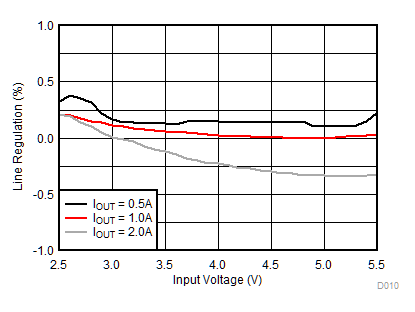
TLV62569 TLV62569P D010_SLVSDG1_TLV62569.gif
VOUT = 1.8 V
Figure 11. Line Regulation
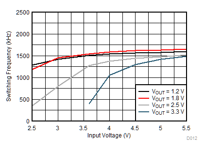
TLV62569 TLV62569P D012_SLVSDG1_TLV62569.gif
IOUT = 1 A
Figure 13. Switching Frequency vs Input Voltage
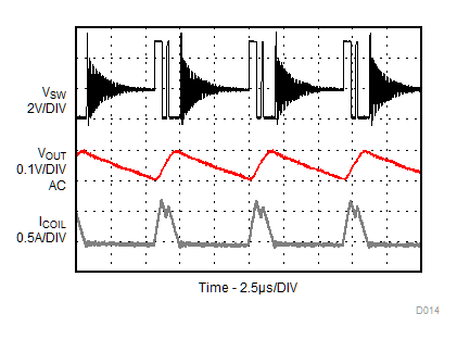
TLV62569 TLV62569P D014_SLVSDG1_TLV62569.gif
IOUT = 0.1 A
Figure 15. Power Save Mode Operation
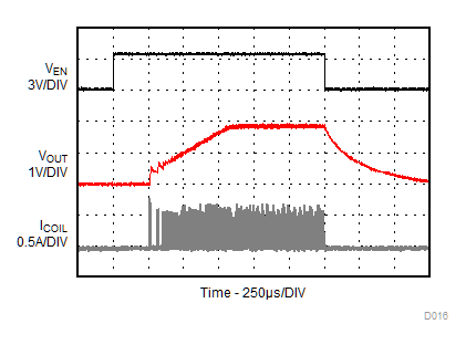
TLV62569 TLV62569P D016_SLVSDG1_TLV62569.gif
IOUT = 0.1 A
Figure 17. Startup and Shutdown with Load
TLV62569 TLV62569P D018_SLVSDG1_TLV62569.gif
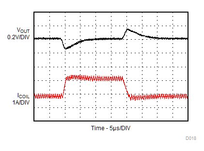
Load Step 0.8 A to 2 A, 1A/μs slew rate C3 = 6.8 pF
Figure 19. Load Transient