ZHCSJS1E September 2008 – September 2019 TLV320AIC3204
PRODUCTION DATA.
- 1 特性
- 2 应用
- 3 描述
- 4 修订历史记录
- 5 Device Comparison Table
- 6 Pin Configuration and Functions
-
7 Specifications
- 7.1 Absolute Maximum Ratings
- 7.2 ESD Ratings
- 7.3 Recommended Operating Conditions
- 7.4 Thermal Information
- 7.5 Electrical Characteristics, ADC
- 7.6 Electrical Characteristics, Bypass Outputs
- 7.7 Electrical Characteristics, Microphone Interface
- 7.8 Electrical Characteristics, Audio DAC Outputs
- 7.9 Electrical Characteristics, LDO
- 7.10 Electrical Characteristics, Misc.
- 7.11 Electrical Characteristics, Logic Levels
- 7.12 I2S LJF and RJF Timing in Master Mode (see )
- 7.13 I2S LJF and RJF Timing in Slave Mode (see )
- 7.14 DSP Timing in Master Mode (see )
- 7.15 DSP Timing in Slave Mode (see )
- 7.16 Digital Microphone PDM Timing (see )
- 7.17 I2C Interface Timing
- 7.18 SPI Interface Timing (See )
- 7.19 Typical Characteristics
- 7.20 Typical Characteristics, FFT
- 8 Parameter Measurement Information
- 9 Detailed Description
- 10Application and Implementation
- 11Power Supply Recommendations
- 12Layout
- 13器件和文档支持
- 14机械、封装和可订购信息
10.2.2.1 Analog Input Connection
The analog inputs to TLV320AIC3204 should be ac-coupled to the device terminals to allow decoupling of signal source's common mode voltage with that of TLV320AIC3204's common mode voltage. The input coupling capacitor in combination with the selected input impedance of TLV320AIC3204 forms a high-pass filter.
For high fidelity audio recording application it is desirable to keep the cutoff frequency of the high pass filter as low as possible. For single-ended input mode, the equivalent input resistance Req can be calculated as
where g is the analog PGA gain calculated in linear terms.
where G is the analog PGA gain programmed in P1_R59-R60 (in dB) and Rin is the value of the resistor programmed in P1_R52-R57 and assumes Rin = Rcm (as defined in P1_R52-R57).
For differential input mode, Req of the half circuit can be calculated as:
where Rin is the value of the resistor programmed in P1_R52-R57, assuming symmetrical inputs.
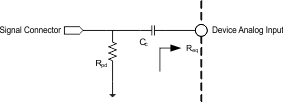
 Figure 22. Analog Input Connection With Pull-down Resistor
 When the analog signal is connected to the system through a connector such as audio jack, it is recommended to put a pull-down resistor on the signal as shown in Figure 22. The pulldown resistor helps keep the signal grounded and helps improve noise immunity when no source is connected to the connector. The pulldown resistor value should be chosen large enough to avoid loading of signal source.
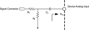
Each analog input of the TLV320AIC3204 is capable of handling signal amplitude of 0.5 Vrms. If the input signal source can drive signals higher than the maximum value, an external resistor divider network as shown in Figure 23 should be used to attenuate the signal to less than 0.5Vrms before connecting the signal to the device. The resistor values of the network should be chosen to provide desired attenuation as well as Equation 6.
 Figure 23. Analog Input Connection With Resistor Divider Network
 Whenever any of the analog input terminals IN1_L, IN2_L, IN3_L, IN1_R, IN2_R or IN3_R are not used in an application, it is recommended to short the unused input terminals together (if convenient) and connect them to ground using a small capacitor (example 0.1 µF).