ZHCSLV0E September 2022 – July 2025 TLV1811 , TLV1812 , TLV1814 , TLV1821 , TLV1822 , TLV1824
PRODMIX
- 1
- 1 特性
- 2 应用
- 3 说明
- 4 引脚配置和功能
- 5 规格
- 6 典型特性
- 7 详细说明
- 8 应用和实施
- 9 器件和文档支持
- 10修订历史记录
- 11机械、封装和可订购信息
封装选项
机械数据 (封装 | 引脚)
散热焊盘机械数据 (封装 | 引脚)
- DSG|8
订购信息
8.1.2.1 具有迟滞功能的反相比较器
具有迟滞功能的反相比较器需要一个以比较器电源电压 (VCC) 为基准的三电阻器网络,如图 8-3 所示。
 图 8-3 采用反相配置且具有迟滞功能的 TLV181x
输出为高电平和低电平时的等效电阻器网络如图 8-3 所示。
 图 8-4 反相配置电阻器等效网络
当 VIN 小于 VA 时,输出电压为高电平(为简单起见,假设 VO 切换至与 VCC 一样高)。三电阻器网络可以表示为 R1 || R3 与 R2 串联,如图 8-4 所示。
下面的方程式 1 定义了从高电平转换到低电平的跳变电压 (VA1)。
方程式 1. 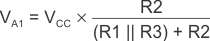
当 VIN 大于 VA 时,输出电压较低。在这种情况下,三电阻器网络可以表示为 R2 || R3 与 R1 串联,如方程式 2 所示。
使用方程式 2 定义从低电平转换到高电平的跳变电压 (VA2)。
方程式 2. 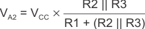
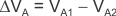
方程式 3 定义了网络提供的总迟滞。
方程式 3.