ZHCSFN0C November   2016  – January 2019 TLV172 , TLV2172 , TLV4172

PRODUCTION DATA.  

  1. 特性
  2. 应用
  3. 说明
    1.     简化原理图
  4. 修订历史记录
  5. Device Comparison Table
  6. Pin Configuration and Functions
    1.     Pin Functions: TLV172
    2.     Pin Functions: TLV2172
    3.     Pin Functions: TLV4172
  7. Specifications
    1. 7.1 Absolute Maximum Ratings
    2. 7.2 ESD Ratings
    3. 7.3 Recommended Operating Conditions
    4. 7.4 Thermal Information: TLV172
    5. 7.5 Thermal Information: TLV2172
    6. 7.6 Thermal Information: TLV4172
    7. 7.7 Electrical Characteristics
    8. 7.8 Typical Characteristics
  8. Detailed Description
    1. 8.1 Overview
    2. 8.2 Functional Block Diagram
    3. 8.3 Feature Description
      1. 8.3.1 Operating Characteristics
      2. 8.3.2 Phase-Reversal Protection
      3. 8.3.3 Electrical Overstress
      4. 8.3.4 Capacitive Load and Stability
    4. 8.4 Device Functional Modes
      1. 8.4.1 Common-Mode Voltage Range
      2. 8.4.2 Overload Recovery
  9. Application and Implementation
    1. 9.1 Application Information
    2. 9.2 Typical Application
      1. 9.2.1 Design Requirements
      2. 9.2.2 Detailed Design Procedure
      3. 9.2.3 Application Curve
  10. 10Power Supply Recommendations
  11. 11Layout
    1. 11.1 Layout Guidelines
    2. 11.2 Layout Example
  12. 12器件和文档支持
    1. 12.1 器件支持
      1. 12.1.1 第三方产品免责声明
      2. 12.1.2 开发支持
        1. 12.1.2.1 TINA-TI™(免费软件下载)
        2. 12.1.2.2 DIP 适配器 EVM
        3. 12.1.2.3 通用运放 EVM
        4. 12.1.2.4 TI 高精度设计
        5. 12.1.2.5 WEBENCH滤波器设计器
    2. 12.2 文档支持
      1. 12.2.1 相关文档
    3. 12.3 相关链接
    4. 12.4 接收文档更新通知
    5. 12.5 社区资源
    6. 12.6 商标
    7. 12.7 静电放电警告
    8. 12.8 术语表
  13. 13机械、封装和可订购信息

封装选项

机械数据 (封装 | 引脚)
散热焊盘机械数据 (封装 | 引脚)
订购信息

Typical Characteristics

at VS = ±18 V, VCM = VS / 2, RLOAD = 10 kΩ connected to VS / 2, and CL = 100 pF (unless otherwise noted)

Table 1. Characteristic Performance Measurements

DESCRIPTION FIGURE
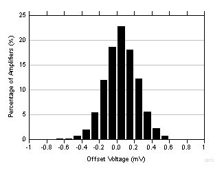
Offset Voltage Production Distribution Figure 1
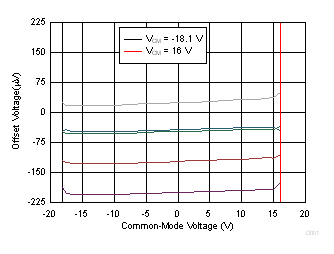
Offset Voltage vs Common-Mode Voltage Figure 2
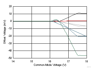
Offset Voltage vs Common-Mode Voltage (Upper Stage) Figure 3
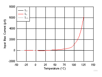
Input Bias Current vs Temperature Figure 4
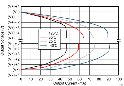
Output Voltage Swing vs Output Current (Maximum Supply) Figure 5
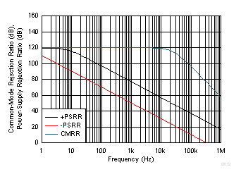
CMRR and PSRR vs Frequency (Referred-to-Input) Figure 6
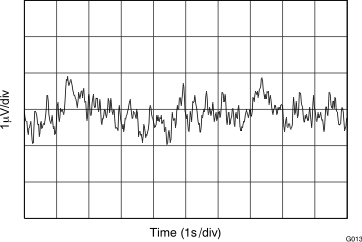
0.1-Hz to 10-Hz Noise Figure 7
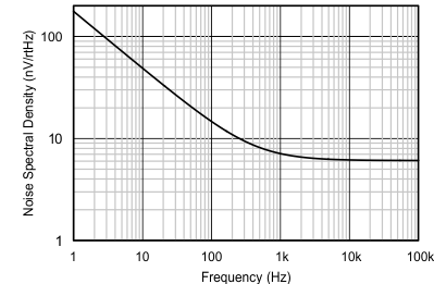
Input Voltage Noise Spectral Density vs Frequency Figure 8
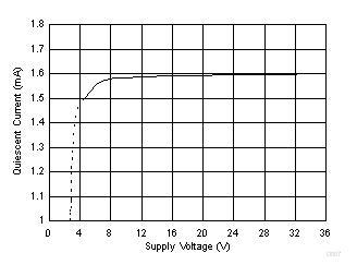
Quiescent Current vs Supply Voltage Figure 9
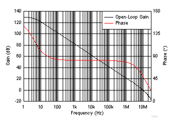
Open-Loop Gain and Phase vs Frequency Figure 10
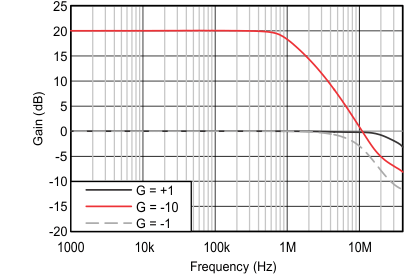
Closed-Loop Gain vs Frequency Figure 11
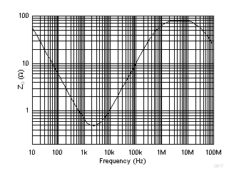
Open-Loop Output Impedance vs Frequency Figure 12
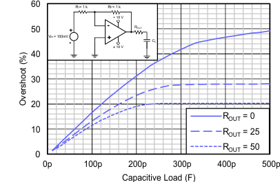
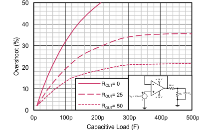
Small-Signal Overshoot vs Capacitive Load Figure 13, Figure 14
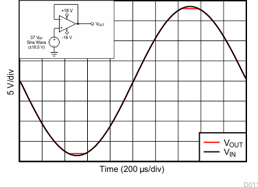
No Phase Reversal Figure 15
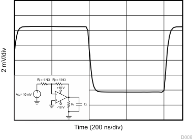
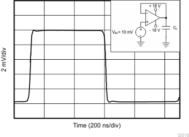
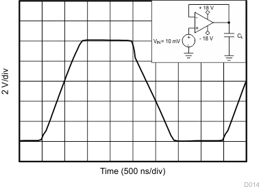
Small-Signal Step Response (10 mV) Figure 16, Figure 17
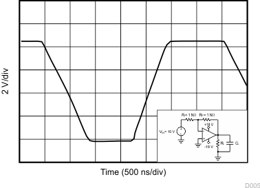
Large-Signal Step Response Figure 18, Figure 19
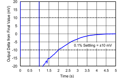
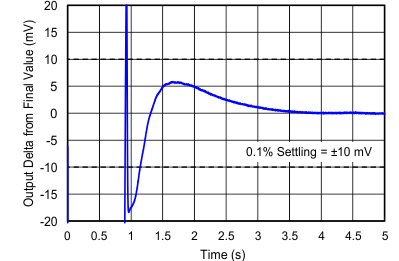
Large-Signal Settling Time Figure 20, Figure 21
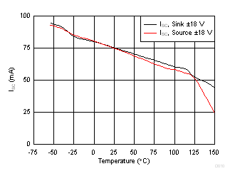
Short-Circuit Current vs Temperature Figure 22
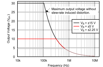
Maximum Output Voltage vs Frequency Figure 23
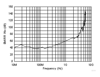
EMIRR IN+ vs Frequency Figure 24
at VS = ±18 V, VCM = VS / 2, RLOAD = 10 kΩ connected to VS / 2, and CL = 100 pF (unless otherwise noted)
TLV172 TLV2172 TLV4172 D013_SBOS784.gif
Distribution taken from 5185 amplifiers
Figure 1. Offset Voltage Production Distribution Histogram
TLV172 TLV2172 TLV4172 D015_SBOS784.gif
5 typical units shown, VS = ±18 V
Figure 3. Offset Voltage vs Common-Mode Voltage
(Upper Stage)
TLV172 TLV2172 TLV4172 D008_SBOS784.gif
Figure 5. Output Voltage Swing vs Output Current (Maximum Supply)
TLV172 TLV2172 TLV4172 G013_BOS557.gif
Figure 7. 0.1-Hz to 10-Hz Noise
TLV172 TLV2172 TLV4172 D007_SBOS784.gif
Figure 9. Quiescent Current vs Supply Voltage
TLV172 TLV2172 TLV4172 figure-11-closed-loop-gain.gif
Figure 11. Closed-Loop Gain vs Frequency
TLV172 TLV2172 TLV4172 C022_correct_graph_SBOS618.gif
100-mV output step, G = –1
Figure 13. Small-Signal Overshoot vs Capacitive Load
TLV172 TLV2172 TLV4172 D011_correct_graph_SBOS784.gif
Figure 15. No Phase Reversal
TLV172 TLV2172 TLV4172 D006_SBOS784.gif
RL = 1 kΩ CL = 10 pF 10-mV step
Figure 17. Small-Signal Step Response
TLV172 TLV2172 TLV4172 D005_SBOS784.gif
RL = 1 kΩ CL = 10 pF
Figure 19. Large-Signal Step Response
TLV172 TLV2172 TLV4172 D023_wrong_graph_SBOS784.gif
10-V negative step G = 1 CL = 10 pF
Figure 21. Large-Signal Settling Time
TLV172 TLV2172 TLV4172 D021_correct_graph_SBOS784.gif
Figure 23. Maximum Output Voltage vs Frequency
TLV172 TLV2172 TLV4172 D001_SBOS784.gif
5 typical units shown, VS = ±18 V
Figure 2. Offset Voltage vs Common-Mode Voltage
TLV172 TLV2172 TLV4172 D009_SBOS784.gif
Figure 4. Input Bias Current vs Temperature
TLV172 TLV2172 TLV4172 D012_SBOS784.gif
Figure 6. CMRR and PSRR vs Frequency (Referred-to-Input)
TLV172 TLV2172 TLV4172 Figure-8-input-voltage.gif
Figure 8. Input Voltage Noise Spectral Density vs Frequency
TLV172 TLV2172 TLV4172 D004_SBOS784.gif
CLOAD = 15 pF
Figure 10. Open-Loop Gain and Phase vs Frequency
TLV172 TLV2172 TLV4172 D017_SBOS784.gif
Figure 12. Open-Loop Output Impedance vs Frequency
TLV172 TLV2172 TLV4172 D023_SBOS784_correct_graph.gif
100-mV output step, G = 1
Figure 14. Small-Signal Overshoot vs Capacitive Load
TLV172 TLV2172 TLV4172 D016_SBOS784.gif
CL = 10 pF 10-mV step
Figure 16. Small-Signal Step Response
TLV172 TLV2172 TLV4172 D014_SBOS784.gif
CL = 10 pF
Figure 18. Large-Signal Step Response
TLV172 TLV2172 TLV4172 D022_SBOS784.gif
10-V positive step G = 1 CL = 10 pF
Figure 20. Large-Signal Settling Time
TLV172 TLV2172 TLV4172 D010_SBOS784.gif
Figure 22. Short-Circuit Current vs Temperature
TLV172 TLV2172 TLV4172 D018_SBOS784.gif
PRF = –10 dBm VSUPPLY = ±18 V VCM = 0 V
Figure 24. EMIRR IN+ vs Frequency