ZHCSBX7D December 2013 – June 2015 TLV1701 , TLV1702 , TLV1704
PRODUCTION DATA.
- 1 特性
- 2 应用范围
- 3 说明
- 4 修订历史记录
- 5 Device Comparison
- 6 Pin Configuration and Functions
- 7 Specifications
- 8 Detailed Description
- 9 Applications and Implementation
- 10Power Supply Recommendations
- 11Layout
- 12器件和文档支持
- 13机械、封装和可订购信息
封装选项
机械数据 (封装 | 引脚)
散热焊盘机械数据 (封装 | 引脚)
订购信息
11 Layout
11.1 Layout Guidelines
Comparators are very sensitive to input noise. For best results, maintain the following layout guidelines:
- Use a printed circuit board (PCB) with a good, unbroken low-inductance ground plane. Proper grounding (use of ground plane) helps maintain specified performance of the TLV170x.
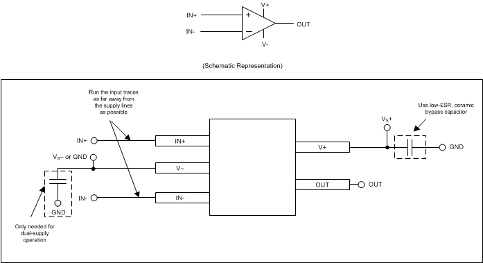
- To minimize supply noise, place a decoupling capacitor (0.1-μF ceramic, surface-mount capacitor) as close as possible to VS as shown in Figure 22.
- On the inputs and the output, keep lead lengths as short as possible to avoid unwanted parasitic feedback around the comparator. Keep inputs away from the output.
- Solder the device directly to the PCB rather than using a socket.
- For slow-moving input signals, take care to prevent parasitic feedback. A small capacitor (1000 pF or less) placed between the inputs can help eliminate oscillations in the transition region. This capacitor causes some degradation to propagation delay when the impedance is low. Run the topside ground plane between the output and inputs.
- Run the ground pin ground trace under the device up to the bypass capacitor, shielding the inputs from the outputs.
11.2 Layout Example
 Figure 22. Comparator Board Layout