SLOS890C October   2015  – December 2019 TLV1701-Q1 , TLV1702-Q1 , TLV1704-Q1

PRODUCTION DATA.  

  1. Features
  2. Applications
  3. Description
    1.     Device Images
      1.      TLV1702-Q1 as a Window Comparator
      2.      Stable Propagation Delay vs Temperature
  4. Revision History
  5. Device Comparison Table
  6. Pin Configuration and Functions
    1.     Pin Functions
  7. Specifications
    1. 7.1 Absolute Maximum Ratings
    2. 7.2 ESD Ratings
    3. 7.3 Recommended Operating Conditions
    4. 7.4 Thermal Information
    5. 7.5 Electrical Characteristics
    6. 7.6 Switching Characteristics
    7. 7.7 Typical Characteristics
  8. Detailed Description
    1. 8.1 Overview
    2. 8.2 Functional Block Diagram
    3. 8.3 Feature Description
      1. 8.3.1 Comparator Inputs
    4. 8.4 Device Functional Modes
      1. 8.4.1 Setting Reference Voltage
  9. Application and Implementation
    1. 9.1 Application Information
    2. 9.2 Typical Application
      1. 9.2.1 Design Requirements
      2. 9.2.2 Detailed Design Procedure
      3. 9.2.3 Application Curve
  10. 10Power Supply Recommendations
  11. 11Layout
    1. 11.1 Layout Guidelines
    2. 11.2 Layout Example
  12. 12Device and Documentation Support
    1. 12.1 Documentation Support
      1. 12.1.1 Related Documentation
    2. 12.2 Related Links
    3. 12.3 Receiving Notification of Documentation Updates
    4. 12.4 Support Resources
    5. 12.5 Trademarks
    6. 12.6 Electrostatic Discharge Caution
    7. 12.7 Glossary
  13. 13Mechanical, Packaging, and Orderable Information

封装选项

机械数据 (封装 | 引脚)
散热焊盘机械数据 (封装 | 引脚)
订购信息

Typical Characteristics

at TA = 25°C, VS = 5 V, RPULLUP = 5.1 kΩ, and input overdrive = 100 mV (unless otherwise noted)
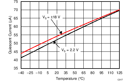
TLV1701-Q1 TLV1702-Q1 TLV1704-Q1 C017_SBOS589.png
Figure 1. Quiescent Current vs Temperature
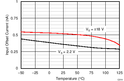
TLV1701-Q1 TLV1702-Q1 TLV1704-Q1 C014_SBOS589.png
Figure 3. Input Offset Current vs Temperature
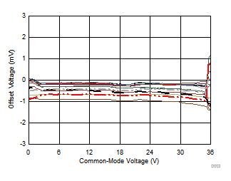
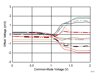
TLV1701-Q1 TLV1702-Q1 TLV1704-Q1 D003_SLOS890.gif
VS = ±18 V 14 typical units shown
Figure 5. Offset Voltage vs Common-Mode Voltage
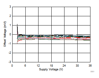
TLV1701-Q1 TLV1702-Q1 TLV1704-Q1 D001_SLOS890.gif
16 typical units shown
Figure 7. Offset Voltage vs Supply Voltage
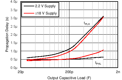
TLV1701-Q1 TLV1702-Q1 TLV1704-Q1 C006_SBOS589.png
Figure 9. Propagation Delay vs Capacitive Load
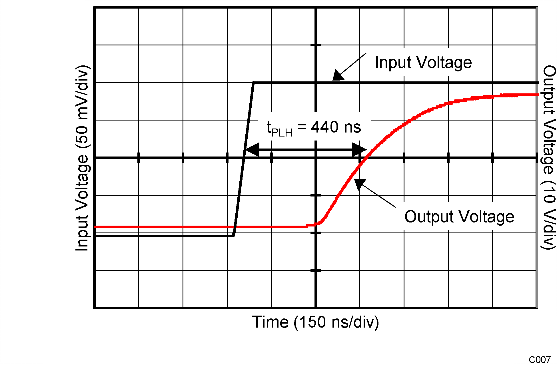
TLV1701-Q1 TLV1702-Q1 TLV1704-Q1 C007_SBOS589.png
VS = 36 V Overdrive = 100 mV
Figure 11. Propagation Delay (TpLH)
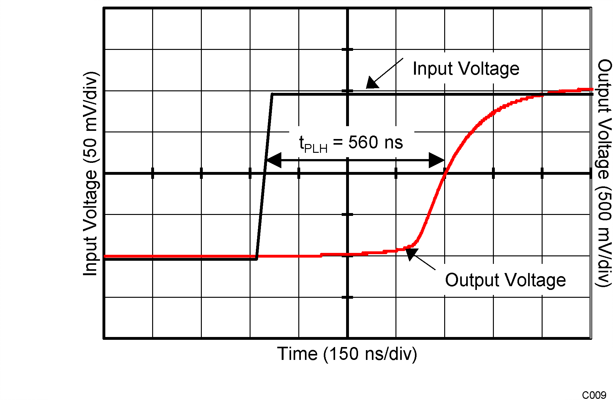
TLV1701-Q1 TLV1702-Q1 TLV1704-Q1 C009_SBOS589.png
VS = 2.2 V Overdrive = 100 mV
Figure 13. Propagation Delay (TpLH)
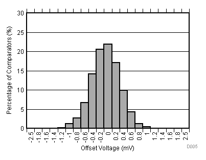
TLV1701-Q1 TLV1702-Q1 TLV1704-Q1 D005_SLOS890.gif
VS = ±18 V Distribution taken from 2524 comparators
Figure 15. Offset Voltage Production Distribution
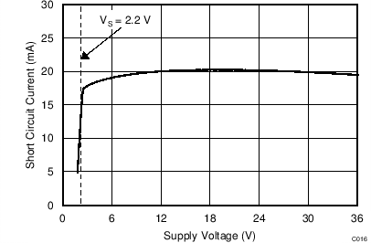
TLV1701-Q1 TLV1702-Q1 TLV1704-Q1 C016_SBOS589.png
Sink current
Figure 17. Short-Circuit Current vs Supply Voltage
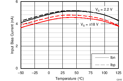
TLV1701-Q1 TLV1702-Q1 TLV1704-Q1 C015_SBOS589.png
Figure 2. Input Bias Current vs Temperature
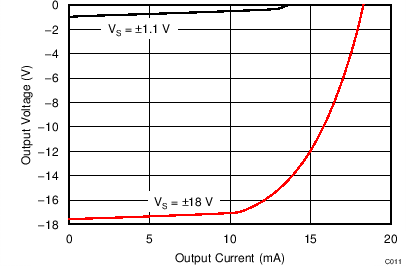
TLV1701-Q1 TLV1702-Q1 TLV1704-Q1 C011_SBOS589.png
Figure 4. Output Voltage vs Output Current
TLV1701-Q1 TLV1702-Q1 TLV1704-Q1 D002_SLOS890.gif
VS = 2.2 V 13 typical units shown
Figure 6. Offset Voltage vs Common-Mode Voltage
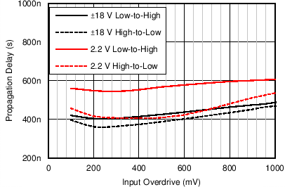
TLV1701-Q1 TLV1702-Q1 TLV1704-Q1 C013_SBOS589.png
Figure 8. Propagation Delay vs Input Overdrive
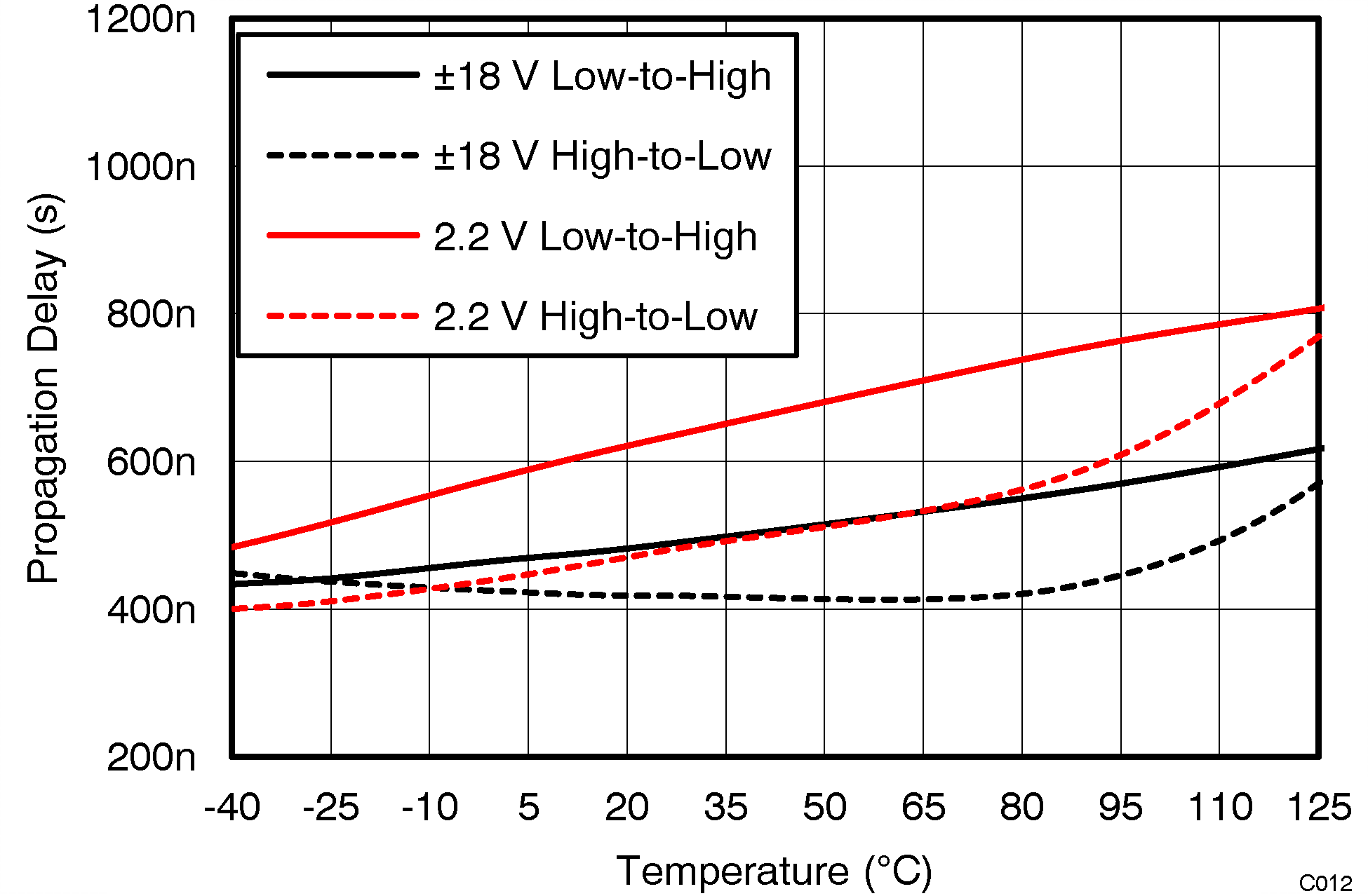
TLV1701-Q1 TLV1702-Q1 TLV1704-Q1 C012_SBOS589.png
VOD = 100 mV
Figure 10. Propagation Delay vs Temperature
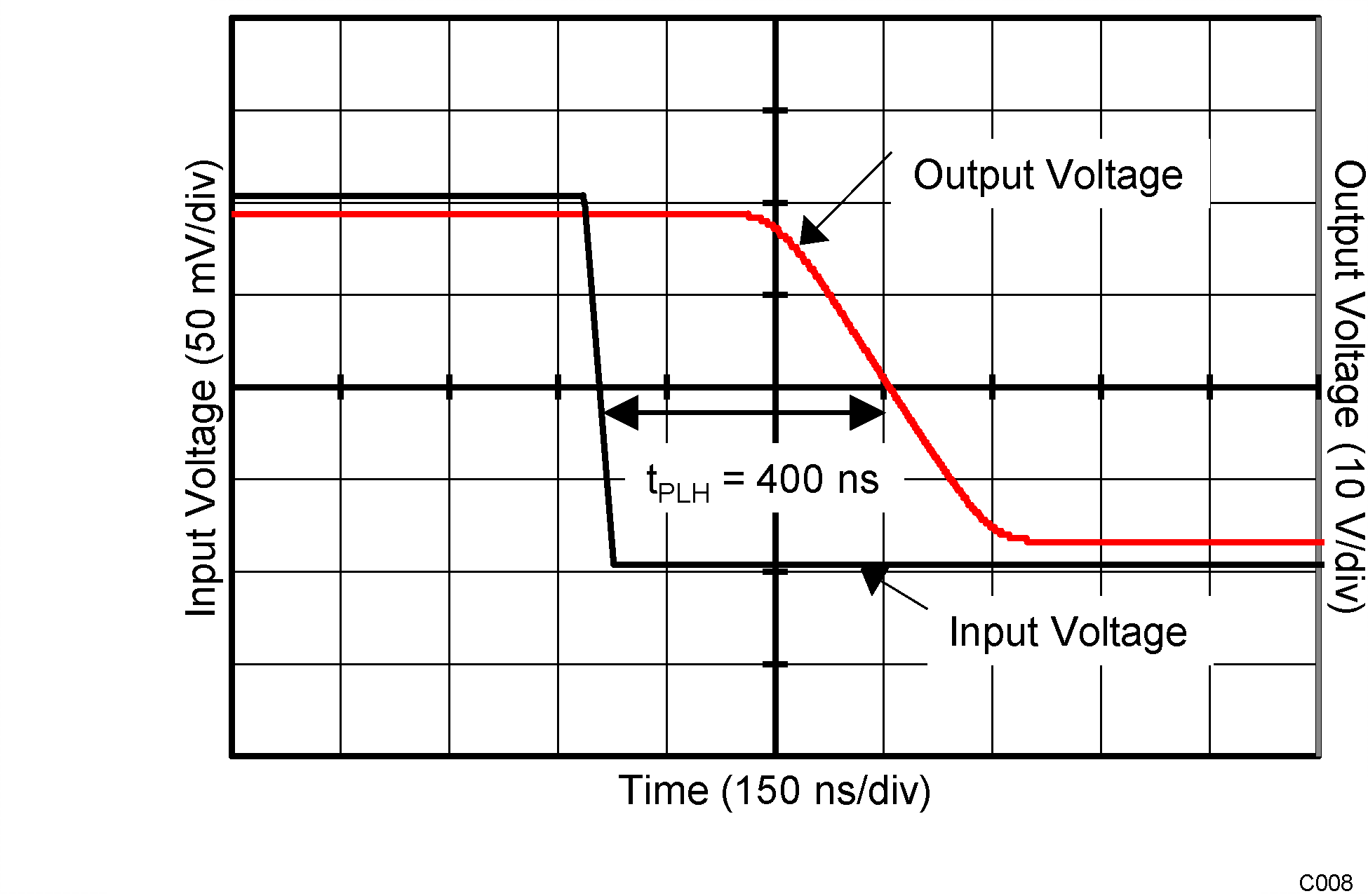
TLV1701-Q1 TLV1702-Q1 TLV1704-Q1 C008_SBOS589.png
VS = 36 V Overdrive = 100 mV
Figure 12. Propagation Delay (TpHL)
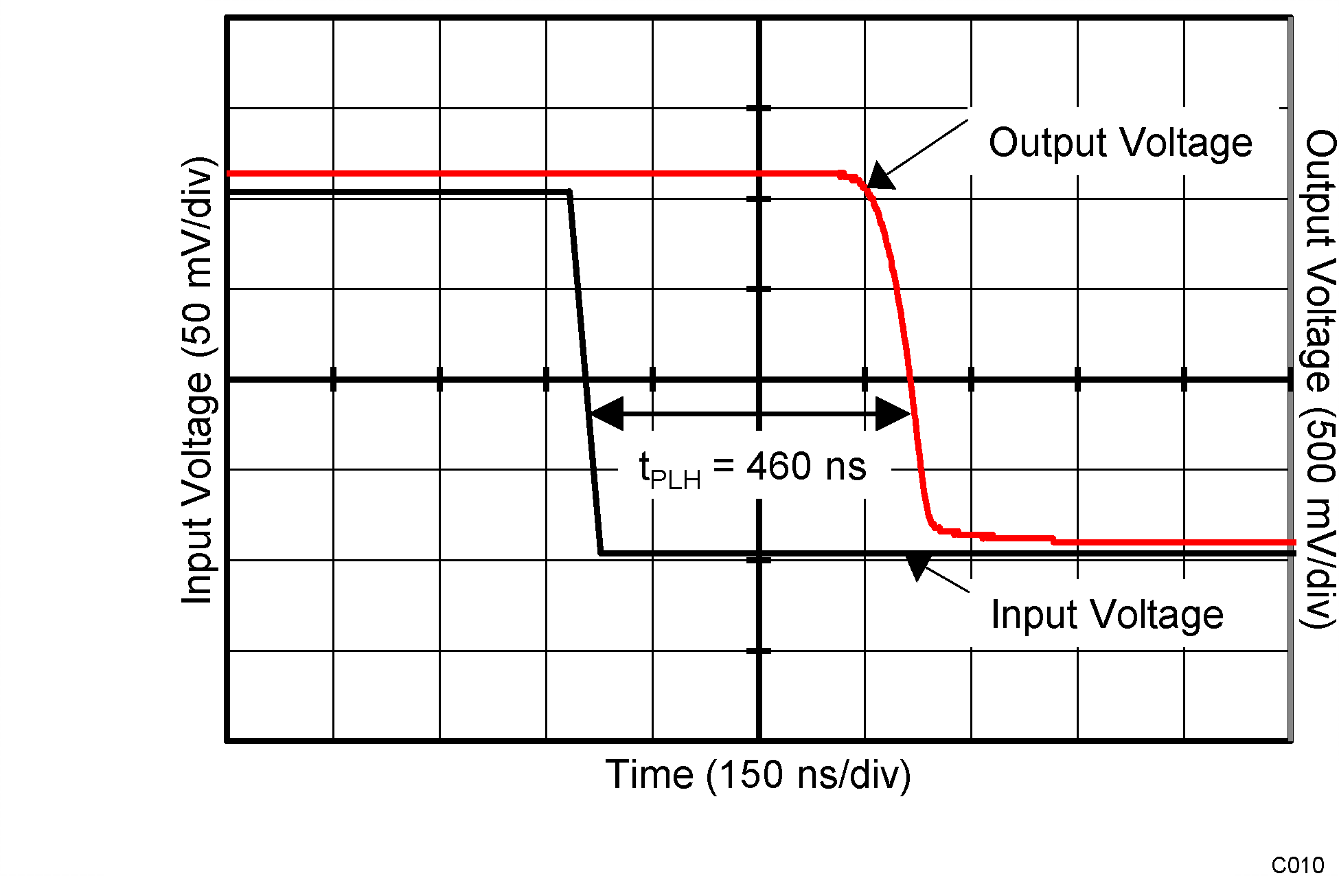
TLV1701-Q1 TLV1702-Q1 TLV1704-Q1 C010_SBOS589.png
VS = 2.2 V Overdrive = 100 mV
Figure 14. Propagation Delay (TpHL)
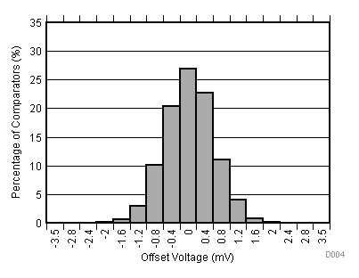
TLV1701-Q1 TLV1702-Q1 TLV1704-Q1 D004_SLOS890.gif
VS = 2.2 V Distribution taken from 2524 comparators
Figure 16. Offset Voltage Production Distribution