SLLSEF8C August 2013 – November 2014 TLK111
PRODUCTION DATA.
- 1 Introduction
- 2 Pin Descriptions
-
3 Hardware Configuration
- 3.1 Bootstrap Configuration
- 3.2 Power Supply Configuration
- 3.3 IO Pins Hi-Z State During Reset
- 3.4 Auto-Negotiation
- 3.5 Auto-MDIX
- 3.6 PHY Address
- 3.7 MII Isolate Mode
- 3.8 Software Strapping Mode
- 3.9 LED Interface
- 3.10 Multi-Configurable LED (MLED)
- 3.11 Loopback Functionality
- 3.12 BIST
- 3.13 Cable Diagnostics
- 4 Interfaces
-
5 Architecture
- 5.1 100Base-TX Transmit Path
- 5.2
100Base-TX Receive Path
- 5.2.1 Analog Front End
- 5.2.2 Adaptive Equalizer
- 5.2.3 Baseline Wander Correction
- 5.2.4 NRZI and MLT-3 Decoding
- 5.2.5 Descrambler
- 5.2.6 5B/4B Decoder and Nibble Alignment
- 5.2.7 Timing Loop and Clock Recovery
- 5.2.8 Phase-Locked Loops (PLL)
- 5.2.9 Link Monitor
- 5.2.10 Signal Detect
- 5.2.11 Bad SSD Detection
- 5.3 10Base-T Receive Path
- 5.4 Auto Negotiation
- 5.5 Link Down Functionality
- 5.6 IEEE 1588 Precision Timing Protocol Support
- 6 Reset and Power Down Operation
- 7 Design Guidelines
-
8 Register Block
- 8.1
Register Definition
- 8.1.1 Basic Mode Control Register (BMCR)
- 8.1.2 Basic Mode Status Register (BMSR)
- 8.1.3 PHY Identifier Register 1 (PHYIDR1)
- 8.1.4 PHY Identifier Register 2 (PHYIDR2)
- 8.1.5 Auto-Negotiation Advertisement Register (ANAR)
- 8.1.6 Auto-Negotiation Link Partner Ability Register (ANLPAR) (BASE Page)
- 8.1.7 Auto-Negotiate Expansion Register (ANER)
- 8.1.8 Auto-Negotiate Next Page Transmit Register (ANNPTR)
- 8.1.9 Auto-Negotiation Link Partner Ability Next Page Register (ANLNPTR)
- 8.1.10 Software Strap Control register 1 (SWSCR1)
- 8.1.11 Software Strap Control register 2 (SWSCR2)
- 8.1.12 Software Strap Control Register 3 (SWSCR3)
- 8.1.13 Extended Register Addressing
- 8.1.14 Fast Link Down Status Register
- 8.1.15 PHY Status Register (PHYSTS)
- 8.1.16 PHY Specific Control Register (PHYSCR)
- 8.1.17 MII Interrupt Status Register 1 (MISR1)
- 8.1.18 MII Interrupt Status Register 2 (MISR2)
- 8.1.19 False Carrier Sense Counter Register (FCSCR)
- 8.1.20 Receiver Error Counter Register (RECR)
- 8.1.21 BIST Control Register (BISCR)
- 8.1.22 RMII Control and Status Register (RCSR)
- 8.1.23 LED Control Register (LEDCR)
- 8.1.24 PHY Control Register (PHYCR)
- 8.1.25 10Base-T Status/Control Register (10BTSCR)
- 8.1.26 BIST Control and Status Register 1 (BICSR1)
- 8.1.27 BIST Control and Status Register2 (BICSR2)
- 8.2 Cable Diagnostic Control Register (CDCR)
- 8.3 PHY Reset Control Register (PHYRCR)
- 8.4 Multi LED Control register (MLEDCR)
- 8.5 IEEE1588 Precision Timing Pin Select (PTPPSEL)
- 8.6 IEEE1588 Precision Timing Configuration (PTPCFG)
- 8.7 TX_CLK Phase Shift Register (TXCPSR)
- 8.8 Power Back Off Control Register (PWRBOCR)
- 8.9 Voltage Regulator Control Register (VRCR)
- 8.10
Cable Diagnostic Configuration/Result Registers
- 8.10.1 ALCD Control and Results 1 (ALCDRR1)
- 8.10.2 Cable Diagnostic Specific Control Registers (CDSCR1 - CDSCR4)
- 8.10.3 Cable Diagnostic Location Results Register 1 (CDLRR1)
- 8.10.4 Cable Diagnostic Location Results Register 2 (CDLRR2)
- 8.10.5 Cable Diagnostic Location Results Register 3 (DDLRR3)
- 8.10.6 Cable Diagnostic Location Results Register 4 (CDLRR4)
- 8.10.7 Cable Diagnostic Location Results Register 5 (CDLRR5)
- 8.10.8 Cable Diagnostic Amplitude Results Register 1 (CDARR1)
- 8.10.9 Cable Diagnostic Amplitude Results Register 2 (CDARR2)
- 8.10.10 Cable Diagnostic Amplitude Results Register 3 (CDARR3)
- 8.10.11 Cable Diagnostic Amplitude Results Register 4 (CDARR4)
- 8.10.12 Cable Diagnostic Amplitude Results Register 5 (CDARR5)
- 8.10.13 Cable Diagnostic General Results Register (CDGRR)
- 8.10.14 ALCD Control and Results 2 (ALCDRR2)
- 8.10.15 ALCD Control and Results 3 (ALCDRR3)
- 8.1
Register Definition
-
9 Electrical Specifications
- 9.1 Absolute Maximum Ratings
- 9.2 Handling Ratings
- 9.3 Recommended Operating ConditionsRedundant row "Power dissipation 200 mW"
- 9.4 48-Pin Industrial Device Thermal Characteristics
- 9.5 48-Pin Extended Temperature (125°C) Device Thermal Characteristics
- 9.6 DC Characteristics, VDD_IO DC Characteristics, SD_IN
- 9.7 DC Characteristics
- 9.8 Power Supply Characteristics
- 9.9
AC Specifications
- 9.9.1 Power Up Timing
- 9.9.2 Reset Timing
- 9.9.3 MII Serial Management Timing
- 9.9.4 100Mb/s MII Transmit Timing
- 9.9.5 100Mb/s MII Receive Timing
- 9.9.6 100Base-TX Transmit Packet Latency Timing
- 9.9.7 100Base-TX Transmit Packet Deassertion Timing
- 9.9.8 100Base-TX Transmit Timing (tR/F and Jitter)
- 9.9.9 100Base-TX Receive Packet Latency Timing
- 9.9.10 100Base-TX Receive Packet Deassertion Timing
- 9.9.11 10Mbs MII Transmit Timing
- 9.9.12 10Mb/s MII Receive Timing
- 9.9.13 10Base-T Transmit Timing (Start of Packet)
- 9.9.14 10Base-T Transmit Timing (End of Packet)
- 9.9.15 10Base-T Receive Timing (Start of Packet)
- 9.9.16 10Base-T Receive Timing (End of Packet)
- 9.9.17 10Mb/s Jabber Timing
- 9.9.18 10Base-T Normal Link Pulse Timing
- 9.9.19 Auto-Negotiation Fast Link Pulse (FLP) Timing
- 9.9.20 100Base-TX Signal Detect Timing
- 9.9.21 100Mbs Loopback Timing
- 9.9.22 10Mbs Internal Loopback Timing
- 9.9.23 RMII Transmit Timing
- 9.9.24 RMII Receive Timing
- 9.9.25 Isolation Timing
- 9.9.26 25MHz_OUT Clock Timing
- 10Revision History, Revision A
2 Pin Descriptions
The TLK111 pins fall into the following interface categories (subsequent sections describe each interface):
|
|
Note: Configuration pin option. See Section 3.1 for Jumper Definitions.
The definitions below define the functionality of each pin.
| Type: I | Input | Type: OD | Open Drain | |
| Type: O | Output | Type: PD, PU | Internal Pulldown/Pullup | |
| Type: I/O | Input/Output | Type: S | Configuration Pin (All configuration pins have weak internal pullups or pulldowns. Use an external 2.2kΩ resistor if you need a different default value. See Section 3.1 for details.) |
2.1 Pin Layout
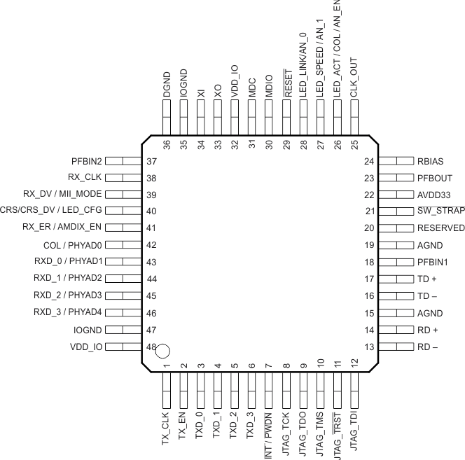
This document describes signals that take on different names depending on configuration. In such cases, the different names are placed together and separated by slash (/) characters. For example, "RXD_3 / PHYAD4". Active low signals are represented by overbars.
2.2 Serial Management Interface (SMI)
| PIN | TYPE | DESCRIPTION | |
|---|---|---|---|
| NAME | NO. | ||
| MDC | 31 | I | MANAGEMENT DATA CLOCK: Clock signal for the management data input/output (MDIO) interface. The maximum MDC rate is 25MHz; there is no minimum MDC rate. MDC is not required to be synchronous to the TX_CLK or the RX_CLK. |
| MDIO | 30 | I/O | MANAGEMENT DATA I/O: Bidirectional command / data signal synchronized to MDC. Either the local controller or the TLK111 may drive the MDIO signal. This pin requires a pull-up resistor with value 2.2kΩ. |
2.3 MAC Data Interface
| PIN | TYPE | DESCRIPTION | |
|---|---|---|---|
| NAME | NO. | ||
| TX_CLK | 1 | O, PD |
MII TRANSMIT CLOCK: MII Transmit Clock provides the 25MHz or 2.5MHz reference clock depending on the speed. Note that in MII mode, this clock has constant phase referenced to REF_CLK. Applications requiring such constant phase may use this feature. Unused in RMII mode. In RMII, X1 reference clock is used as the clock for both transmit and receive. |
| TX_EN | 2 | I, PD | TRANSMIT ENABLE: TX_EN is presented on the rising edge of the TX_CLK . TX_EN indicates the presence of valid data inputs on TXD[3:0] in MII mode, and on TXD [1:0] in the RMII mode. TX_EN is an active high signal. |
| TXD_0 TXD_1 TXD_2 TXD_3 |
3
4 5 6 |
I, PD | TRANSMIT DATA: In MII mode, the transmit data nibble received from the MAC is synchronous to the rising edge of the TX_CLK signal. In RMII mode, TXD [1:0] received from the MAC is synchronous to the 50MHz reference clock on XI. |
| RX_CLK | 38 | O | RECEIVE CLOCK: In MII mode it is the receive clock that provides either a 25MHz or 2.5MHz reference clock, depending on the speed, that is derived from the received data stream. |
| RX_DV / MII_MODE | 39 | S, O, PD | RECEIVE DATA VALID: This pin indicates valid data is present on the RXD [3:0] for MII mode or on RXD [1:0] for RMII mode, independently from Carrier Sense. |
| RX_ER / AMDIX_EN | 41 | S, O, PU | RECEIVE ERROR: This pin indicates that an error symbol has been detected within a received packet in both MII and RMII mode. In MII mode, RX_ER is asserted high synchronously to RX_CLK and in RMII mode, synchronously to XI (50MHz). This pin is not required to be used by the MAC, in either MII or RMII, because the PHY is corrupting data on a receive error. |
| RXD_0 / PHYAD1 RXD_1 / PHYAD2 RXD_2 / PHYAD3 RXD_3 / PHYAD4 |
43
44 45 46 |
S, O, PD | RECEIVE DATA: Symbols received on the cable are decoded and presented on these pins synchronous to RX_CLK. They contain valid data when RX_DV is asserted. A nibble RXD [3:0] is received in the MII mode and 2-bits RXD[1:0] is received in the RMII Mode. PHY address pins PHYAD[4:1] are multiplexed with RXD [3:0], and are pulled down. PHYAD0 (LSB of the address) is multiplexed with COL on pin 42, and is pulled up. If no external pullup/pulldown is present, the default address is 0x01. |
| CRS / LED_CFG | 40 | S, O, PU |
CARRIER SENSE: In MII mode this pin is asserted high when the receive medium is non-idle. CARRIER SENSE/RECEIVE DATA VALID: In RMII mode, this pin combines the RMII Carrier and Receive Data Valid indications. |
| COL / PHYAD0 | 42 | S, O, PU |
COLLISION DETECT: For MII mode in Full Duplex Mode this pin is always low. In 10Base-T/100Base-TX half-duplex modes, this pin is asserted HIGH only when both transmit and receive media are non-idle. This pin is not used in RMII mode. |
2.4 10Mbs and 100Mbs PMD Interface
| PIN | TYPE | DESCRIPTION | |
|---|---|---|---|
| NAME | NO. | ||
| TD–, TD+ | 16, 17 | I/O | Differential common driver transmit output (PMD Output Pair): These differential outputs are automatically configured to either 10Base-T or 100Base-TX signaling. In Auto-MDIX mode of operation, this pair can be used as the Receive Input pair. These pins require 3.3V bias for operation. |
| RD–, RD+ | 13, 14 | I/O | Differential receive input (PMD Input Pair): These differential inputs are automatically configured to accept either 100Base-TX or 10Base-T signaling. In Auto-MDIX mode of operation, this pair can be used as the Transmit Output pair. These pins require 3.3V bias for operation. |
2.5 Clock Interface
| PIN | TYPE | DESCRIPTION | |
|---|---|---|---|
| NAME | NO. | ||
| XI | 34 | I | CRYSTAL/OSCILLATOR INPUT: |
| MII reference clock: Reference clock. 25MHz ±50ppm-tolerance crystal reference or oscillator input. The device supports either an external crystal resonator connected across pins XI and XO, or an external CMOS-level oscillator source connected to pin XI only. | |||
| RMII reference clock: Primary clock reference input for the RMII mode. The input must be connected to a 50MHz ±50ppm-tolerance CMOS-level oscillator source. | |||
| XO | 33 | O | CRYSTAL OUTPUT: Reference Clock output. XO pin is used for crystal only. This pin should be left floating when an oscillator input is connected to XI. |
| CLKOUT | 25 | O | CLOCK OUTPUT: In MII mode, this pin provides a 25 MHz clock output to the system. In RMII mode, this pin provides a 50MHz clock output. This feature allows other devices to use the reference clock from the TLK111 without requiring additional clock sources. |
2.6 LED Interface
(See Table 3-3 for LED Mode Selection)| PIN | TYPE | DESCRIPTION | ||
|---|---|---|---|---|
| NAME | NO. | |||
| LED_LINK / AN_0 | 28 | S, O, PU | LED Pin to indicate status | |
| Mode 1 | LINK Indication LED: Indicates the status of the link. When the link is good, the LED is ON. | |||
| Mode 2 and Mode 3 | ACT indication LED: Indicates transmit and receive activity in addition to the status of the Link. The LED is ON when Link is good. The LED blinks when the transmitter or receiver is active. | |||
| LED_SPEED / AN_1 | 27 | S, O, PU | LED Pin to indicate the speed of the link. SPEED Indication LED indicates whether the link is 100Mb/s or 10Mb/s. The LED is ON when the link speed is 100Mbs and OFF when it is 10Mbs. | |
| LED_ACT / AN_EN | 26 | S, O, PU | LED Pin to indicate status. | |
| Mode 1 | ACT indication LED: Indicates if there is any activity on the link. The LED is ON (pulse) when activity is present on either Transmit or Receive channel. | |||
| Mode 2 | COL indication LED: Indicates collision detection. | |||
| Mode 3 | may be programmed to DUPLEX Indication LED and indicates Full-duplex status. | |||
2.7 JTAG Interface
| PIN | TYPE | DESCRIPTION | |
|---|---|---|---|
| NAME | NO. | ||
| JTAG_TCK | 8 | I, PU | JTAG Test Clock: This pin has a weak internal pullup. |
| JTAG_TDI | 12 | I, PU | JTAG Test Data Input: This pin has a weak internal pullup. |
| JTAG_TDO | 9 | O | JTAG Test Data Output |
| JTAG_TMS | 10 | I, PU | JTAG Test Mode Select: This pin has a weak internal pullup. |
| JTAG_TRST | 11 | I, PU | JTAG Reset: This pin is an active-low asynchronous test reset with a weak internal pullup. |
2.8 Reset and Power Down
| PIN | TYPE | DESCRIPTION | |
|---|---|---|---|
| NAME | NO. | ||
| RESET | 29 | I, PU | This pin is an active-low reset input that initializes or re-initializes all the internal registers of the TLK111. Asserting this pin low for at least 1µs will force a reset process to occur. All jumper options are reinitialized as well. |
| INT / PWDN | 7 | IO, OD, PU | Register access is required for this pin to be configured either as power down or as an interrupt. The default function of this pin is power down. |
| When this pin is configured for a power down function, an active low signal on this pin places the device in power down mode. | |||
| When this pin is configured as an interrupt pin, then this pin is asserted low when an interrupt condition occurs. The pin has an open-drain output with a weak internal pull-up. Some applications may require an external pull-up resistor. | |||
2.9 Power and Bias Connections
| PIN | TYPE | DESCRIPTION | |
|---|---|---|---|
| NAME | NO. | ||
| RBIAS | 24 | I | Bias Resistor Connection: Use a 4.87kΩ 1% resistor connected from RBIAS to GND. |
| PFBOUT | 23 | O | Power Feedback Output: Place 10µf and 0.1μF capacitors (ceramic preferred) close to PFBOUT. |
| In single-supply operation, connect this pin to PFBIN1 and PFBIN2 (pin 18 and pin 37). See Figure 3-1 for proper placement. | |||
| In multiple supply operation, this pin is not used. | |||
| PFBIN1 | 18 | I | Power Feedback Input: These pins are fed with power from PFBOUT (pin 23) in single supply operation. |
| PFBIN2 | 37 | In multiple supply operation, connect a 1.55V external power supply to these pins. Connect a small capacitor of 0.1µF close to each pin. To power down the internal linear regulator, write to register 0x00d0. | |
| VDD_IO | 32, 48 | P | I/O 3.3V, 2.5V, or 1.8V Supply - For details, see Section 3.2.3 |
| IOGND | 35, 47 | P | I/O ground |
| DGND | 36 | P | Digital ground |
| AVDD33 | 22 | P | Analog 3.3V power supply |
| AGND | 15, 19 | P | Analog ground |
| RESERVED | 20 | I/O | RESERVED: This pin must be pulled-up through 2.2kΩ resistor to AVDD33 supply. |