ZHCSIO0A December 2017 – August 2018 TLC6C5724-Q1
PRODUCTION DATA.
- 1 特性
- 2 应用
- 3 说明
- 4 修订历史记录
- 5 Pin Configuration and Functions
- 6 Specifications
-
7 Detailed Description
- 7.1 Overview
- 7.2 Functional Block Diagram
- 7.3
Feature Description
- 7.3.1 Maximum Constant-Sink-Current Setting
- 7.3.2 Brightness Control and Dot Correction
- 7.3.3 Grayscale Configuration
- 7.3.4
Diagnostics
- 7.3.4.1 LED Diagnostics
- 7.3.4.2 Adjacent-Pin-Short Check
- 7.3.4.3 IREF Short and IREF Open Detection
- 7.3.4.4 Pre-Thermal Warning Flag
- 7.3.4.5 Thermal Error Flag
- 7.3.4.6 Negate Bit Toggle
- 7.3.4.7 LOD_LSD Self-Test
- 7.3.4.8 ERR Pin
- 7.3.4.9 ERROR Clear
- 7.3.4.10 Global Reset
- 7.3.4.11 Slew Rate Control
- 7.3.4.12 Channel Group Delay
- 7.4 Device Functional Modes
- 7.5 Programming
- 7.6 Register Maps
- 8 Application and Implementation
- 9 Power Supply Recommendations
- 10Layout
- 11器件和文档支持
- 12机械、封装和可订购信息
7.3.2 Brightness Control and Dot Correction
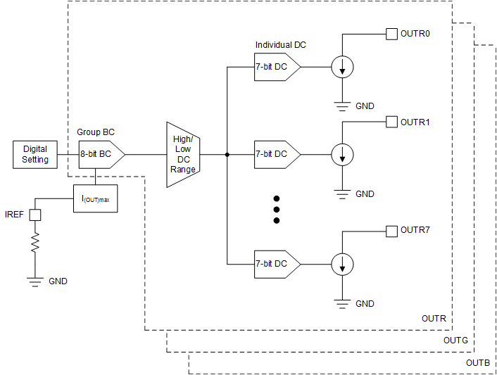
The TLC6C5724-Q1 device implements an 8-bit group brightness control (BC) and 7-bit individual dot correction (DC) to calibrate the output current. The 24 output channels are divided into three groups: OUTRn, OUTGn, and OUTBn. Each group contains 8 output channels. There are two configurable ranges for the DC value of each group. One is the low DC range with output current from 0 to 66.7% I(OUT)max. The other is the high DC range with output current from 33.3% I(OUT)max to 100% I(OUT)max. The IREF resistor, BC, DC, and DC range together determine the channel output current, as shown in Figure 21. Equation 2 and Equation 3 are the detailed output current calculation formulas.
Equation 2 determines the output sink current for each color group when DC is in the high adjustment range.

Equation 3 determines the output sink current for each color group when DC is in the low adjustment range.

 Figure 21. Brightness Control and Dot Correction Block Diagram