SBVS146D August 2010 – December 2015 TLC5971
PRODUCTION DATA.
- 1 Features
- 2 Applications
- 3 Description
- 4 Revision History
- 5 Pin Configuration and Functions
- 6 Specifications
- 7 Parametric Measurement Information
-
8 Detailed Description
- 8.1 Overview
- 8.2 Functional Block Diagram
- 8.3 Feature Description
- 8.4 Device Functional Modes
- 8.5 Programming
- 9 Application and Implementation
- 10Power Supply Recommendations
- 11Layout
- 12Device and Documentation Support
- 13Mechanical, Packaging, and Orderable Information
封装选项
机械数据 (封装 | 引脚)
散热焊盘机械数据 (封装 | 引脚)
订购信息
9 Application and Implementation
NOTE
Information in the following applications sections is not part of the TI component specification, and TI does not warrant its accuracy or completeness. TI’s customers are responsible for determining suitability of components for their purposes. Customers should validate and test their design implementation to confirm system functionality.
9.1 Application Information
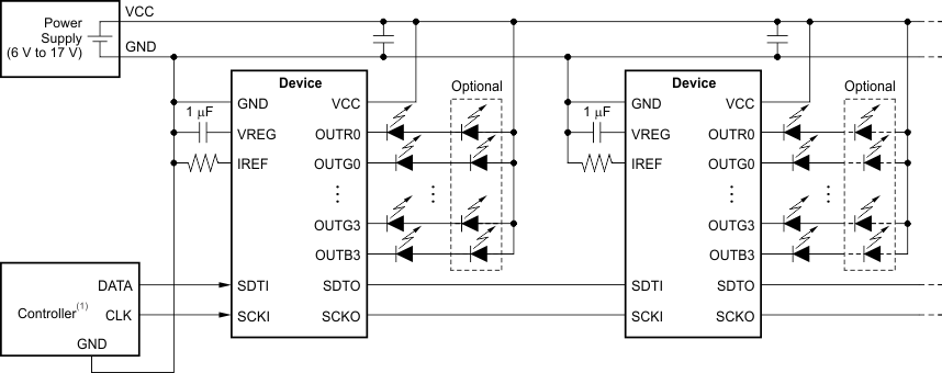
The device is a 12-channel, constant sink current, LED driver. This device can be connected in series to drive many LED lamps with only a few controller ports. Functional control data and PWM control data can be written from the SDI and SCK input terminal. The PWM timing reference clock can be chosen from the internal oscillation or external SCK signal.
9.2 Typical Application
9.2.1 Design Requirements
For this design example, use Table 6 as the input parameters.
Table 6. Design Parameters
| DESIGN PARAMETER | EXAMPLE VALUE | |||
|---|---|---|---|---|
| VCC Input Voltage Range | 3 V to 5.5 V | |||
| LED Lamp (VLED) Input Voltage Range | Maximum 17 V | |||
| SIN, SCLK, LAT and GSCLK Voltage Range | Low Level = GND, High Level = VCC | |||
9.2.2 Detailed Design Procedure
9.2.2.1 Define Basic Parameters
To begin the design process, a few parameters must be decided as following"
- Maximum output constant-current value for each color LED lamp
- Maximum LED forward voltage (Vf) and maximum VLED
- Total LEDs and Cascaded IC Number
9.2.2.2 Data Input Sequence
224-bit data packets are sent through single-wire interface for the PWM control of three output channels. Select the BC data, FC data and write the GS data to the register following the signal timing.
9.2.2.3 How to Control the TLC5971
To set each function mode, BC color, GS output, 6-bit write command, 5-bit FC data, 21-bit BC data for each color group, and 192-bit GS data for OUTXn, a total number of 224 bits must be written into the device. Figure 32 shows the 224-bit data packet configuration.
When N units of the TLC5971 are cascaded (as shown in Figure 33), N × 224 bits must be written from the controller into the first device to control all devices. The number of cascaded devices is not limited as long as the proper voltage is supplied to the device at VCC. The packets for all devices must be written again whenever the data in one packet is changed.
 Figure 32. 224-Bit Data Packet Configuration
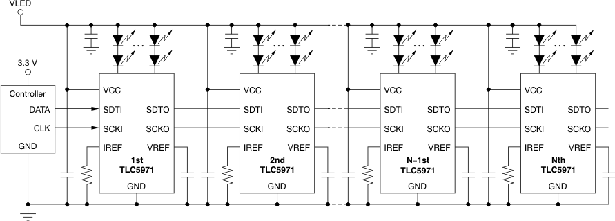 Figure 33. Cascading Connection of N TLC5971 Units
9.2.2.3.1 Data Write and PWM Control with Internal Grayscale Clock Mode
When the EXTCLK bit is 0, the internal oscillator clock is used for PWM control of OUTXn (X = R/G/B and n = 0-3) as the GS reference clock. This mode is ideal for illumination applications that change the display image at low frequencies. The data and clock timing is shown in Figure 3 and Figure 34. A writing procedure for the function setting and display control follows:
- Power up VCC (VLED); all OUTXn are off because BLANK is set to 1.
- Write the 224-bit data packet (with MSB bit first) for the Nth TLC5971 using the SDTI and SCKI signals. The first six bits of the 224-bit data packet are used as the write command. The write command must be 25h (100101b); otherwise, the 218-bit data in the 224-bit shift register are not copied to the 218-bit data latch. The EXTCLK bit must be set to 0 for the internal oscillator mode. Also, the DSPRPT bit should be set to 1 to repeat the PWM timing control and BLANK set to 0 to start the PWM control.
- Write the 224-bit data packet for the (N – 1) TLC5971 without delay after step 2.
- Repeat the data write sequence until all TLC5971s have data. The total shift clock count (SCKI) is now 224 × N. After all device data are written, stop the SCKI at a high or low level for 8× the period between the last SCKI rising edge and the second to last SCKI rising edge. Then the 218 LSBs in the 224-bit shift resister are copied to the 218-bit data latch in all devices and the PWM control is started or updated at the same time.
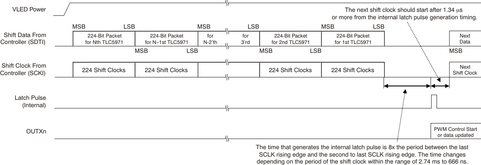 Figure 34. Data Packet and Display Start/Update Timing 1 (Internal Oscillator Mode)
9.2.2.3.2 Data Write and PWM Control with External Grayscale Clock Mode
When the EXTCLK bit is 1, the data shift clock (SCKI) is used for PWM control of OUTXn (X = R/G/B and n = 0-3) as the GS reference clock. This mode is ideal for video image applications that change the display image with high frequencies or for certain display applications that must synchronize all TLC5971s. The data and clock timing are shown in Figure 3 and Figure 35. A writing procedure for the display data and display timing control follows:
- Power up VCC (VLED); all OUTXn are off because BLANK is set to 1.
- Write the 224-bit data packet MSB-first for the Nth TLC5971 using the SDTI and SCKI signals. The first six bits of the 224-bit data packet are used as the write command. The write command must be 25h (100101b); otherwise, the 218-bit data in the 224-bit shift register are not copied to the 218-bit data latch. The EXTCLK bit must be set to 1 for the external oscillator mode. Also, the DSPRPT bit should be set to 0 so that the PWM control is not repeated, the TMGRST bit should be set to 1 to reset the PWM control timing at the internal latch pulse generation, and BLANK must be set to 0 to start the PWM control.
- Write the 224-bit data for the (N – 1) TLC5971 without delay after step 2.
- Repeat the data write sequence until all TLC5971s have data. The total shift clock count (SCKI) is 224 × N. After all device data are written, stop the SCKI at a high or low level for 8× the period between the last SCKI rising edge and the second to last SCKI rising edge. Then the 218 LSBs in the 224-bit shift resister are copied to the 218-bit data latch in all devices.
- To start the PWM control, send one pulse of the SCKI clock with SDTI low after 1.34 µs or more from step 4. The OUTXn are turned on when the output GS data are not 0000h.
- Send the remaining 65535 SCKI clocks with SDTI low. Then the PWM control for OUTXn is synchronized with the SCKI clock and one display period is finished with a total of 65536 SCKI clock periods.
- Repeat step 2 to step 6 for the next display period.
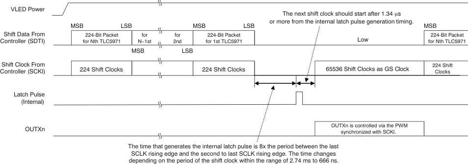 Figure 35. Data Packet and Display Start/Update Timing 2 (External Clock Mode)
There is another control procedure that is recommended for a long chain of cascaded devices. The data and clock timings are shown in Figure 3 and Figure 36. When 256 TLC5971 units are cascaded, use the following procedure:
- Power up VCC (VLED); all OUTXn are off because BLANK is set to 1.
- Write the 224-bit data packet MSB-first for the 256th TLC5971 using the SDTI and SCKI signals. The EXTCLK bit must be set to 1 for the external oscillator mode. Also, the DSPRPT bit should be set to 0 so that the PWM control does not repeat, the TMGRST bit should be set to 1 to reset the PWM control timing with the internal latch pulse, and BLANK must be set to 0 to start the PWM control.
- Repeat the data write sequence for all TLC5971s. The total shift clock count (SCKI) is 57344 (224 × 256). After all device data are written, stop the SCKI signal at a high or low level for eight or more periods between the last SCKI rising edge and the second to last SCKI rising edge. Then the 218 LSBs in the 224-bit shift resister are copied to the 218-bit data latch in all devices.
- To control the PWM, send 8192 SCKI clock periods with SDTI low after 1.34 µs or more from step 3 (or step 7). These 8192 clock periods are used for the OUTXn PWM control.
- Write the new 224-bit data packets to the 256th to first TLC5971s for the next display with 256 × 224 SCKI clock for a total of 57344 clocks. The PWM control for OUTXn remains synchronized with the SCKI clock and one display period is finished with a total of 65536 SCKI clocks. The SCKI clock signal is therefore used for PWM control and, at the same time, to write data into the shift registers of all cascaded parts.
- Stop the SCKI signal at a high or low level for eight or more periods between the last SCKI rising edge and the second to last SCKI rising edge. Then the 218-bit LSBs in the 224-bit shift resister are copied to the 218-bit data latch in all devices.
- Repeat step 4 to step 6 for the next display periods.
 Figure 36. Data Packet and Display Start/Update Timing 3
(External Clock Mode With 256 Cascaded Devices)
9.2.3 Application Curve
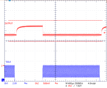 Figure 37. Output Waveform With GS Data Latch Input
