SLDS165A December 2008 – December 2014 TLC5941-Q1
PRODUCTION DATA.
- 1 Features
- 2 Applications
- 3 Description
- 4 Revision History
- 5 Pin Configuration and Functions
- 6 Specifications
- 7 Parameter Measurement Information
- 8 Detailed Description
- 9 Application and Implementation
- 10Power Supply Recommendations
- 11Layout
- 12Device and Documentation Support
- 13Mechanical, Packaging, and Orderable Information
封装选项
机械数据 (封装 | 引脚)
- PWP|28
散热焊盘机械数据 (封装 | 引脚)
- PWP|28
订购信息
8 Detailed Description
8.1 Overview
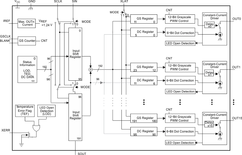
The TLC5941-Q1 device is a 16-channel constant-current sink LED driver with individual PWM dimming and dot correction, designed for LEDs in automotive indicator application. Each channel has up to 60-mA capability, giving a combined 960-mA current capability when paralleled. A single external resistor sets the maximum current value of all 16 channels.
The TLC5941-Q1 device can adjust 4096-step grayscale brightness of each channel OUTn individually, using a PWM control scheme. As well, the TLC5941-Q1 device has the capability to fine-adjust 64-step the output current of each channel independently. The dot correction adjusts the brightness variations between LED channels and other LED drivers. Both grayscale control and dot correction are accessible via a serial interface, which can be connected to microcontrollers or digital signal processors in various ways.
The integrated diagnostic circuit is used to detect device working condition, normal operation, LOD or TEF. The LED open detection (LOD) indicates a broken or disconnected LED at an output terminal. The thermal error flag (TEF) indicates an over temperature condition.
8.2 Functional Block Diagram
8.3 Feature Description
8.3.1 Serial Interface
The TLC5941-Q1 device has a flexible serial interface, which can be connected to microcontrollers or digital signal processors in various ways. Only 3 pins are needed to input data into the device. The rising edge of SCLK signal shifts the data from the SIN pin to the internal register. After all data is clocked in, a high-level pulse of XLAT signal latches the serial data to the internal registers. The internal registers are level-triggered latches of XLAT signal. All data are clocked in with the MSB first. The length of serial data is 96 bit or 192 bit, depending on the programming mode. Grayscale data and dot correction data can be entered during a grayscale cycle. Although new grayscale data can be clocked in during a grayscale cycle, the XLAT signal should only latch the grayscale data at the end of the grayscale cycle. Latching in new grayscale data immediately overwrites the existing grayscale data. Figure 12 shows the timing chart. More than two TLC5941-Q1 devices can be connected in series by connecting an SOUT pin from one device to the SIN pin of the next device. An example of cascading two TLC5941-Q1 devices is shown in Figure 13. The SOUT pin can also be connected to the controller to receive status information from TLC5941-Q1 device as shown in Figure 18.
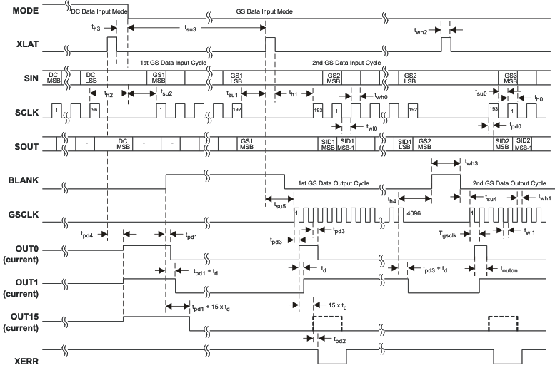 Figure 12. Serial Data Input Timing Chart
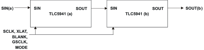 Figure 13. Cascading Two TLC5941-Q1 Devices
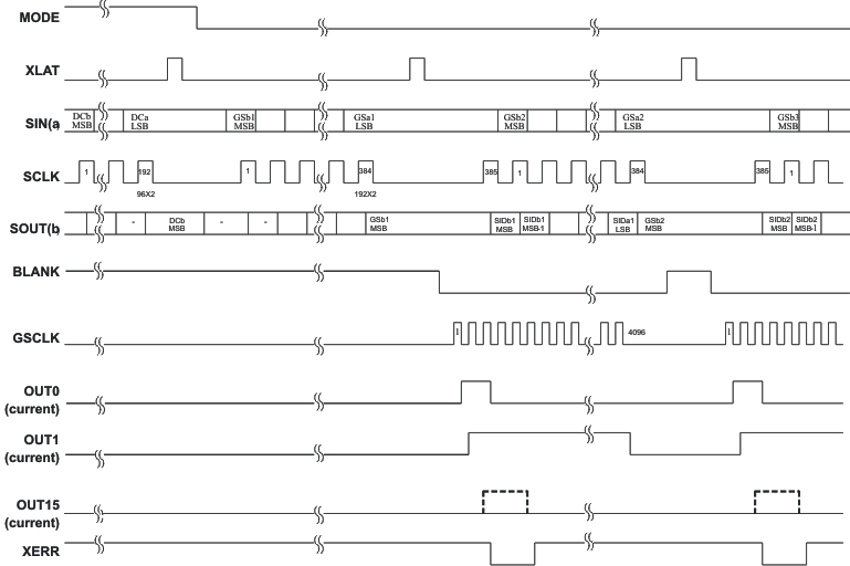 Figure 14. Timing Chart for Two Cascaded TLC5941-Q1 Devices
8.3.2 Error Information Output
The open-drain output XERR is used to report both of the TLC5941-Q1 error flags, TEF and LOD. During normal operating conditions, the internal transistor connected to the XERR pin is turned off. The voltage on XERR is pulled up to VCC through an external pullup resistor. If TEF or LOD is detected, the internal transistor is turned on, and XERR is pulled to GND. Because XERR is an open-drain output, multiple ICs can be ORed together and pulled up to VCC with a single pullup resistor which reduces the number of signals needed to report a system error (see Figure 18).
To differentiate LOD and TEF signal from XERR pin, LOD can be masked out with BLANK = HIGH.
Table 1. XERR Truth Table
| ERROR CONDITION | ERROR INFORMATION | SIGNALS | |||
|---|---|---|---|---|---|
| TEMPERATURE | OUTn VOLTAGE | TEF | LOD | BLANK | XERR |
| TJ < T(TEF) | Don't Care | L | X | H | H |
| TJ > T(TEF) | Don't Care | H | X | L | |
| TJ < T(TEF) | OUTn > V(LED) | L | L | L | H |
| OUTn < V(LED) | L | H | L | ||
| TJ > T(TEF) | OUTn > V(LED) | H | L | L | |
| OUTn < V(LED) | H | H | L | ||
8.3.3 TEF: Thermal Error Flag
The TLC5941-Q1 device provides a temperature error flag (TEF) circuit to indicate an overtemperature condition of the IC. If the junction temperature exceeds the threshold temperature (160°C typical), the TEF flag becomes H and XERR pin goes to low level. When the junction temperature becomes lower than the threshold temperature, the TEF flag becomes L and the XERR pin becomes high impedance. The TEF status can also be read out from the TLC5941-Q1 status register.
8.3.4 LOD: LED Open Detection
The TLC5941-Q1 device has an LED-open detection circuit that detects broken or disconnected LEDs. The LED open detector pulls the XERR pin to GND when an open LED is detected. The XERR pin and the corresponding error bit in the Status Information Data is only active under the following open LED conditions:
- OUTn is on and the time tpd2 (1 μs typical) has passed.
- The voltage of OUTn is < 0.3V (typical)
The LOD status of each output can be also read out from the SOUT pin. See the Status Information Output section for details. The LOD error bits are latched into the Status Information Data when the XLAT pin returns to a low after a high. Therefore, the XLAT pin must be pulsed high then low while the XERR pin is active in order to latch the LOD error into the Status Information Data for subsequent reading via the serial shift register.
8.3.5 Delay Between Outputs
The TLC5941-Q1 device has graduated delay circuits between outputs. These circuits can be found in the constant current driver block of the device (see the functional block diagram). The fixed-delay time is 20 ns (typical), the OUT0 output has no delay, the OUT1 output has 20-ns delay, the OUT2 output has 40-ns delay, and so on. The maximum delay is 300 ns from the OUT0 output to the OUT15 output. The delay works during switch on and switch off of each output channel. These delays prevent large inrush currents which reduces the bypass capacitors when the outputs turn on.
8.3.6 Output Enable
All OUTn channels of the TLC5941-Q1 device can be switched off with one signal. When the BLANK signal is set high, all OUTn channels are disabled, regardless of logic operations of the device. The grayscale counter is also reset. When the BLANK signal is set low, all OUTn channels work under normal conditions. If BLANK goes low and then back high again in less than 300 ns, all outputs programmed to turn on still turn on for either the programmed number of grayscale clocks, or the length of time that the BLANK signal was low, which ever is lower. For example, if all outputs are programmed to turn on for 1 ms, but the BLANK signal is only low for 200 ns, all outputs still turn on for 200 ns, even though some outputs are turning on after the BLANK signal has already gone high.
Table 2. BLANK Signal Truth Table
| BLANK | OUT0 to OUT15 |
|---|---|
| LOW | Normal condition |
| HIGH | Disabled |
8.3.7 Status Information Output
The TLC5941-Q1 device does have a status information register, which can be accessed in grayscale mode (MODE = GND). After the XLAT signal latches the data into the GS register, the input shift register data is replaced with status information data (SID) of the device (see Figure 22). The LOD, TEF, and dot-correction register data can be read out at the SOUT pin. The status information data packet is 192 bits wide. Bits 0 through 15 contain the LOD status of each channel. Bit 16 contains the TEF status. Bits 24 through 119 contain the data of the dot-correction register. The remaining bits are reserved. The complete status information data packet is shown in Figure 15.
The SOUT pin outputs the MSB of the SID at the same time the SID are stored in the SID register, as shown in Figure 16. The next SCLK pulse, which is the clock for receiving the MSB of the next grayscale data, transmits MSB-1 of SID. If output voltage is < 0.3 V (typical) when the output sink current turns on, the LOD status flag becomes active. The LOD status flag is an internal signal which pulls the XERR pin down to low when the LOD status flag becomes active. The delay time, tpd2 (1 μs, maximum), is from the time of turning on the output sink current to the time the LOD status flag becomes valid. The timing for each channels LOD status to become valid is shifted by the 30-ns (maximum), channel-to-channel turn-on time. After the first GSCLK pin goes high, the OUT0 LOD status is valid; tpd3 + tpd2 = 60 ns + 1 μs = 1.06 μs. The OUT1 LOD status is valid; tpd3 + td + tpd2 = 60 ns + 30 ns + 1 μs = 1.09 μs. The OUT2 LOD status is valid; tpd3 + 2td + tpd2 = 1.12 μs, and so on. The total time from the first GSCLK rising edge until all LOD become valid is about 1.51 μs maximum (tpd3 + 15td + tpd2); tsuLOD must be > 1.51 μs (see Figure 16) to ensure that all LOD data are valid.
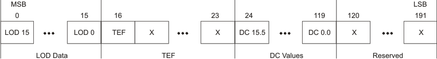 Figure 15. Status Information Data Packet Format
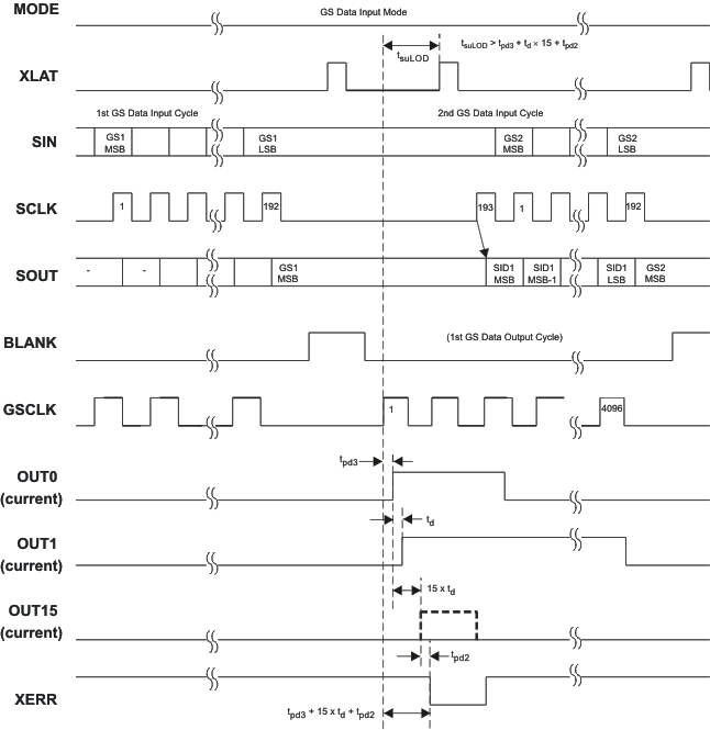 Figure 16. Readout Status Information Data (SID) Timing Chart
The LOD status of each output can be read out from the SOUT pin. The LOD error bits are latched into the Status Information Data when the XLAT pin returns to a low after a high. Therefore, the XLAT pin must be pulsed high then low while the XERR pin is active in order to latch the LOD error into the Status Information Data for subsequent reading through the serial shift register.
8.3.8 Grayscale PWM Operation
The grayscale PWM cycle begins with the falling edge of BLANK. The first GSCLK pulse after the BLANK pin goes low increases the grayscale counter by one and switches on all OUTn pins with grayscale value not zero. Each following rising edge of the GSCLK pin increases the grayscale counter by one. The TLC5941-Q1 device compares the grayscale value of each output, OUTn, with the grayscale counter value. All OUTn pins with grayscale values equal to the counter values are switched off. A BLANK = H signal after 4096 GSCLK pulses resets the grayscale counter to zero and completes the grayscale PWM cycle (see Figure 17). When the counter reaches a count of FFFh, the counter stops counting and all outputs turn off. Pulling the BLANK pin high before the counter reaches FFFh immediately resets the counter to zero.
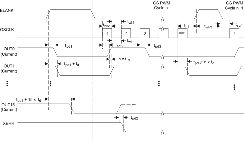 Figure 17. Grayscale PWM Cycle Timing Chart
8.3.8.1 Output On Time
The amount of time that each output is turned on is a function of the grayscale clock frequency and the programmed grayscale PWM value. The on-time of each output can be calculated using Equation 6.
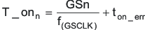
where
- T_onn is the time that the OUTn pin turns on and sinks current
- GSn is the programmed grayscale PWM value of the OUTn pin between 0 and 4095
- ton_err is the output on time error defined in the Switching Characteristics table
When using Equation 6 with very high GSCLK frequencies and very low grayscale PWM values, the resulting T_on time may be negative. If T_on is negative, the output does not turn on. For example, using f(GSCLK) = 30 MHz, GSn = 1, and the typical ton_err = 50 nS, Equation 6 calculates that OUTn turns on for –16.6 ns. This output may not turn on under these conditions. Increasing the PWM value or reducing the GSCLK clock frequency ensures turn-on.
8.4 Device Functional Modes
8.4.1 Operating Modes
The TLC5941-Q1 device has two operating modes defined by MODE as shown in Table 3. The GS and DC registers are set to random values that are not known just after power on. The GS and DC values must be programmed before turning on the outputs.
NOTE
When initially setting GS and DC data after power on, the GS data must be set before the DC data is set. Failure to set GS data before DC data may result in the first bit of GS data being lost. The XLAT pin must be low when the MODE pin goes high-to-low or low-to-high to change back and forth between GS mode and DC mode.
Table 3. TLC5941-Q1 Operating Modes Truth Table
| MODE | INPUT SHIFT REGISTER | OPERATING MODE |
|---|---|---|
| GND | 192 bit | Grayscale PWM Mode |
| VCC | 96 bit | Dot Correction Data Input Mode |