SLVS867B May 2009 – August 2015 TLC59213 , TLC59213A
PRODUCTION DATA.
- 1 Features
- 2 Applications
- 3 Description
- 4 Revision History
- 5 Pin Configuration and Functions
- 6 Specifications
- 7 Parameter Measurement Information
- 8 Detailed Description
- 9 Application and Implementation
- 10Power Supply Recommendations
- 11Layout
- 12Device and Documentation Support
- 13Mechanical, Packaging, and Orderable Information
6 Specifications
6.1 Absolute Maximum Ratings(1)
over operating free-air temperature range (unless otherwise noted)| MIN | MAX | UNIT | |||
|---|---|---|---|---|---|
| VDD | Supply voltage | –0.5 | 15 | V | |
| VI | Input voltage | –0.5 | VCC + 0.5 | V | |
| Collector-emitter voltage | –0.5 | 15 | V | ||
| IO | Peak output current | –500 | mA | ||
| IIK | Input clamp current | VI < 0 V | –20 | mA | |
| IOK | Output clamp current | VO < 0 V | –500 | mA | |
| Tstg | Storage temperature | –65 | 150 | °C | |
(1) Stresses beyond those listed under Absolute Maximum Ratings may cause permanent damage to the device. These are stress ratings only, which do not imply functional operation of the device at these or any other conditions beyond those indicated under Recommended Operating Conditions. Exposure to absolute-maximum-rated conditions for extended periods may affect device reliability.
6.2 ESD Ratings
| VALUE | UNIT | |||
|---|---|---|---|---|
| V(ESD) | Electrostatic discharge | Human body model (HBM), per ANSI/ESDA/JEDEC JS-001(1) | ±2000 | V |
| Charged-device model (CDM), per JEDEC specification JESD22-C101(2) | ±1000 | |||
(1) JEDEC document JEP155 states that 500-V HBM allows safe manufacturing with a standard ESD control process.
(2) JEDEC document JEP157 states that 250-V CDM allows safe manufacturing with a standard ESD control process.
6.3 Recommended Operating Conditions
| MIN | MAX | UNIT | ||||
|---|---|---|---|---|---|---|
| VCC | Supply voltage | 4.5 | 13.2 | V | ||
| VIH | High-level input voltage | 2 | V | |||
| VIL | Low-level input voltage | 0.8 | V | |||
| IO | Output current (8 channel) | N package | Duty cycle < 10% | 400 | mA | |
| Duty cycle < 50% | 200 | |||||
| PW package | Duty cycle < 10% | 350 | ||||
| Duty cycle < 50% | 170 | |||||
| TA | Operating free-air temperature | –40 | 85 | °C | ||
6.4 Electrical Characteristics
over recommended operating free-air temperature range (unless otherwise noted)| PARAMETER | TEST CONDITIONS | MIN | TYP | MAX | UNIT | ||
|---|---|---|---|---|---|---|---|
| ICEX | Output leakage current | VCC = 13.2 V, Outputs off | 2 | µA | |||
| VCE(sus) | Output saturation voltage | IOUT = –350 mA | 2.35 | V | |||
| IOUT = –225 mA | 2.15 | ||||||
| IOUT = –100 mA | 1.96 | ||||||
| II | Input current | VCC = 13.2 V, VI = 0 or 13.2 V | 1 | µA | |||
| Vf | Clamp forward voltage | If = –350 mA | –2 | V | |||
| ICC | Supply current | VCC = 13.2 V, VI = 0 or 13.2 V |
All outputs OFF | 4.6 | 13 | mA | |
| All outputs ON | 4.8 | 13 | |||||
| CI | Input capacitance | 10 | pF | ||||
6.5 Timing Requirements
over recommended operating free-air temperature range (unless otherwise noted), see Figure 3| MIN | MAX | UNIT | |||||
|---|---|---|---|---|---|---|---|
| tsu | Setup time | D before CLK ↑ | 50 | ns | |||
| CLR high before CLK ↑ | 50 | ns | |||||
| th | Hold time | D after CLK ↑ | TLC59213, TLC59213A | TA = -40°C to 85°C | 50 | ns | |
| TLC59213 | TA = 0°C to 70°C | 25 | |||||
| TLC59213A | TA = 0°C to 70°C, VCC = 4.5 V to 5.5 V | 15 | |||||
| TA = 0°C to 70°C, VCC = 10.8 V to 13.2 V | 19 | ||||||
| tw | Pulse width | CLK, CLR | 100 | ns | |||
6.6 Switching Characteristics
over operating free-air temperature range (unless otherwise noted), see Figure 3| PARAMETER | FROM (INPUT) |
TO (OUTPUT) |
TEST CONDITIONS |
TA = 25°C | TA = –40°C to 85°C | UNIT | ||||
|---|---|---|---|---|---|---|---|---|---|---|
| MIN | TYP | MAX | MIN | MAX | ||||||
| tPLH | Propagation delay time, low-to-high level output |
CLK | Y | RL = 25 Ω, CL = 15 pF |
107 | 200 | 250 | ns | ||
| tPHL | Propagation delay time, high-to-low level output |
CLK | Y | RL = 25 Ω, CL = 15 pF |
111 | 200 | 250 | ns | ||
| tPHLR | Propagation delay time, high-to-low level output |
CLR | Y | RL = 25 Ω, CL = 15 pF |
104 | 200 | 250 | ns | ||
6.7 Typical Characteristics
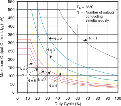
 Figure 1. Maximum Output Current vs Duty Cycle (TSSOP (PW) Package)
 Figure 2. Maximum Output Current vs Duty Cycle (DIP (N) Package)