SLOS984 June   2017 TLC2272AM-MIL

PRODUCTION DATA.  

  1. Features
  2. Applications
  3. Description
  4. Revision History
  5. Pin Configuration and Functions
  6. Specifications
    1. 6.1 Absolute Maximum Ratings
    2. 6.2 ESD Ratings
    3. 6.3 Recommended Operating Conditions
    4. 6.4 Thermal Information
    5. 6.5 TLC2272AM-MIL Electrical Characteristics VDD = 5 V
    6. 6.6 TLC2272AM-MIL Electrical Characteristics VDD± = ±5 V
    7. 6.7 Typical Characteristics
  7. Detailed Description
    1. 7.1 Overview
    2. 7.2 Functional Block Diagram
    3. 7.3 Feature Description
    4. 7.4 Device Functional Modes
  8. Application and Implementation
    1. 8.1 Application Information
      1. 8.1.1 Macromodel Information
    2. 8.2 Typical Application
      1. 8.2.1 High-Side Current Monitor
        1. 8.2.1.1 Design Requirements
        2. 8.2.1.2 Detailed Design Procedure
          1. 8.2.1.2.1 Differential Amplifier Equations
        3. 8.2.1.3 Application Curves
  9. Power Supply Recommendations
  10. 10Layout
    1. 10.1 Layout Guidelines
    2. 10.2 Layout Example
  11. 11Device and Documentation Support
    1. 11.1 Receiving Notification of Documentation Updates
    2. 11.2 Community Resources
    3. 11.3 Trademarks
    4. 11.4 Electrostatic Discharge Caution
    5. 11.5 Glossary
  12. 12Mechanical, Packaging, and Orderable Information

封装选项

机械数据 (封装 | 引脚)
散热焊盘机械数据 (封装 | 引脚)
订购信息

Layout

Layout Guidelines

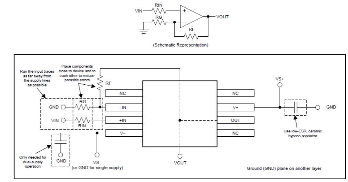
The TLC2272AM-MIL device is a wideband amplifier. To realize the full operational performance of the device, good high-frequency printed-circuit-board (PCB) layout practices are required. Low-loss 0.1-μF bypass capacitors must be connected between each supply pin and ground as close to the device as possible. The bypass capacitor traces should be designed for minimum inductance.

Layout Example

TLC2272AM-MIL Layout Example.gif Figure 57. Layout Example