ZHCSJX7A June   2019  – December 2019 TLA2518

PRODUCTION DATA.  

  1. 特性
  2. 应用
  3. 说明
    1.     Device Images
      1.      TLA2518 方框图和 应用
  4. 修订历史记录
  5. Pin Configuration and Functions
    1.     Pin Functions
  6. Specifications
    1. 6.1 Absolute Maximum Ratings
    2. 6.2 ESD Ratings
    3. 6.3 Recommended Operating Conditions
    4. 6.4 Thermal Information
    5. 6.5 Electrical Characteristics
    6. 6.6 Timing Requirements
    7. 6.7 Switching Characteristics
    8. 6.8 Typical Characteristics
  7. Detailed Description
    1. 7.1 Overview
    2. 7.2 Functional Block Diagram
    3. 7.3 Feature Description
      1. 7.3.1 Multiplexer and ADC
      2. 7.3.2 Reference
      3. 7.3.3 ADC Transfer Function
      4. 7.3.4 ADC Offset Calibration
      5. 7.3.5 Programmable Averaging Filter
      6. 7.3.6 General-Purpose I/Os
      7. 7.3.7 Oscillator and Timing Control
      8. 7.3.8 Output Data Format
      9. 7.3.9 Device Programming
        1. 7.3.9.1 Enhanced-SPI Interface
        2. 7.3.9.2 Register Read/Write Operation
          1. 7.3.9.2.1 Register Write
          2. 7.3.9.2.2 Register Read
    4. 7.4 Device Functional Modes
      1. 7.4.1 Device Power-Up and Reset
      2. 7.4.2 Manual Mode
      3. 7.4.3 On-the-Fly Mode
      4. 7.4.4 Auto-Sequence Mode
    5. 7.5 TLA2518 Registers
      1. 7.5.1  SYSTEM_STATUS Register (Address = 0x0) [reset = 0x81]
        1. Table 9. SYSTEM_STATUS Register Field Descriptions
      2. 7.5.2  GENERAL_CFG Register (Address = 0x1) [reset = 0x0]
        1. Table 10. GENERAL_CFG Register Field Descriptions
      3. 7.5.3  DATA_CFG Register (Address = 0x2) [reset = 0x0]
        1. Table 11. DATA_CFG Register Field Descriptions
      4. 7.5.4  OSR_CFG Register (Address = 0x3) [reset = 0x0]
        1. Table 12. OSR_CFG Register Field Descriptions
      5. 7.5.5  OPMODE_CFG Register (Address = 0x4) [reset = 0x0]
        1. Table 13. OPMODE_CFG Register Field Descriptions
      6. 7.5.6  PIN_CFG Register (Address = 0x5) [reset = 0x0]
        1. Table 14. PIN_CFG Register Field Descriptions
      7. 7.5.7  GPIO_CFG Register (Address = 0x7) [reset = 0x0]
        1. Table 15. GPIO_CFG Register Field Descriptions
      8. 7.5.8  GPO_DRIVE_CFG Register (Address = 0x9) [reset = 0x0]
        1. Table 16. GPO_DRIVE_CFG Register Field Descriptions
      9. 7.5.9  GPO_VALUE Register (Address = 0xB) [reset = 0x0]
        1. Table 17. GPO_VALUE Register Field Descriptions
      10. 7.5.10 GPI_VALUE Register (Address = 0xD) [reset = 0x0]
        1. Table 18. GPI_VALUE Register Field Descriptions
      11. 7.5.11 SEQUENCE_CFG Register (Address = 0x10) [reset = 0x0]
        1. Table 19. SEQUENCE_CFG Register Field Descriptions
      12. 7.5.12 CHANNEL_SEL Register (Address = 0x11) [reset = 0x0]
        1. Table 20. CHANNEL_SEL Register Field Descriptions
      13. 7.5.13 AUTO_SEQ_CH_SEL Register (Address = 0x12) [reset = 0x0]
        1. Table 21. AUTO_SEQ_CH_SEL Register Field Descriptions
  8. Application and Implementation
    1. 8.1 Application Information
    2. 8.2 Typical Applications
      1. 8.2.1 Mixed-Channel Configuration
        1. 8.2.1.1 Design Requirements
        2. 8.2.1.2 Detailed Design Procedure
          1. 8.2.1.2.1 Digital Input
          2. 8.2.1.2.2 Digital Open-Drain Output
          3. 8.2.1.2.3 Application Curve
      2. 8.2.2 Digital Push-Pull Output Configuration
  9. Power Supply Recommendations
    1. 9.1 AVDD and DVDD Supply Recommendations
  10. 10Layout
    1. 10.1 Layout Guidelines
    2. 10.2 Layout Example
  11. 11器件和文档支持
    1. 11.1 接收文档更新通知
    2. 11.2 社区资源
    3. 11.3 商标
    4. 11.4 静电放电警告
    5. 11.5 Glossary
  12. 12机械、封装和可订购信息

封装选项

机械数据 (封装 | 引脚)
散热焊盘机械数据 (封装 | 引脚)
订购信息

Typical Characteristics

at TA = 25°C, AVDD = 5 V, DVDD = 1.8 V, and fSAMPLE = 1 MSPS (unless otherwise noted)
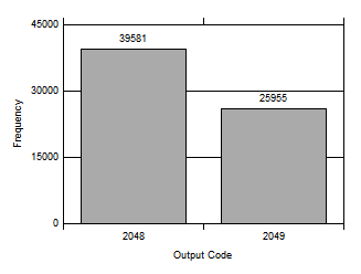
TLA2518 C001_SBAS979.gif
Standard deviation = 0.49 LSB
Figure 3. DC Input Histogram
TLA2518 C002_SBAS979_SBAS980.gif
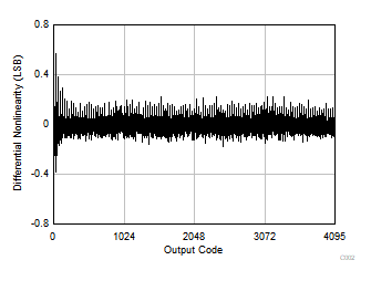
Typical DNL = ±0.5 LSB
Figure 5. Typical DNL
TLA2518 C003_SBAS980.gif
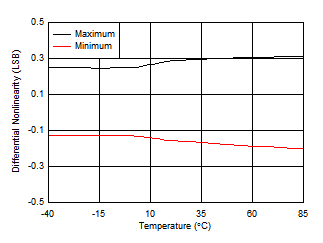
Figure 7. DNL vs Temperature
TLA2518 C018_SBAS979_SBAS980.gif
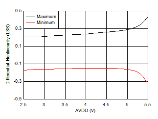
Figure 9. DNL vs AVDD
TLA2518 C006_SBAS980.gif
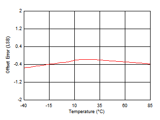
Figure 11. Offset Error vs Temperature
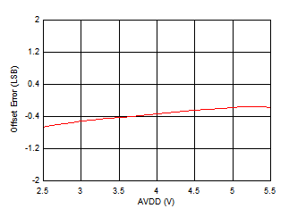
TLA2518 C016_SBAS979_SBAS980.gif
Figure 13. Offset Error vs AVDD
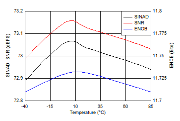
TLA2518 C009_SBAS980.gif
Figure 15. Noise Performance vs Temperature
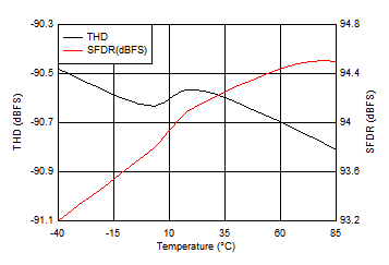
TLA2518 C011_SBAS980.gif
Figure 17. Distortion Performance vs Temperature
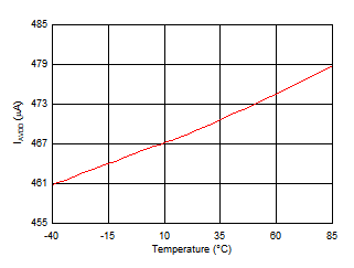
TLA2518 C013_SBAS980.gif
Figure 19. Analog Supply Current vs Temperature
TLA2518 C015_SBAS979_SBAS980.gif
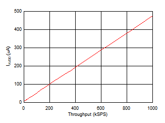
Figure 21. Analog Supply Current vs Throughput
TLA2518 C008_SBAS979_SBAS980.gif
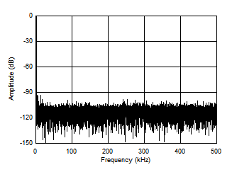
fIN = 2 kHz, SNR = 73.2 dB, THD = –92.1 dB
Figure 4. Typical FFT
TLA2518 C004_SBAS979_SBAS980.gif
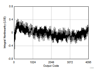
Typical INL = ±0.5 LSB
Figure 6. Typical INL
TLA2518 C005_SBAS980.gif
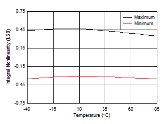
Figure 8. INL vs Temperature
TLA2518 C019_SBAS979_SBAS980.gif
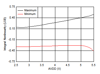
Figure 10. INL vs AVDD
TLA2518 C007_SBAS980.gif
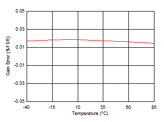
Figure 12. Gain Error vs Temperature
TLA2518 C017_SBAS979_SBAS980.gif
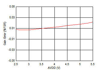
Figure 14. Gain Error vs AVDD
TLA2518 C010_SBAS979_SBAS980.gif
Figure 16. Noise Performance vs AVDD
TLA2518 C012_SBAS979_SBAS980.gif
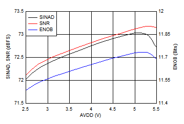
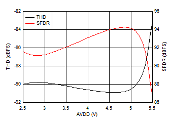
Figure 18. Distortion Performance vs AVDD
TLA2518 C014_SBAS979_SBAS980.gif
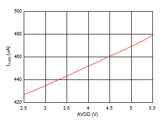
Figure 20. Analog Supply Current vs AVDD