SLVSA79A April 2010 – September 2016 TL1963A-Q1
PRODUCTION DATA.
- 1 Features
- 2 Applications
- 3 Description
- 4 Revision History
- 5 Pin Configuration and Functions
- 6 Specifications
- 7 Detailed Description
- 8 Application and Implementation
- 9 Power Supply Recommendations
- 10Layout
- 11Device and Documentation Support
- 12Mechanical, Packaging, and Orderable Information
10 Layout
10.1 Layout Guidelines
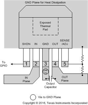
For best performance, follow the guidelines below:
- All traces must be as short as possible.
- Use wide traces for IN, OUT, and GND to minimize the parasitic electrical effects.
- A minimum output capacitor of 10 µF with an ESR of 3 Ω or less is recommended to prevent oscillations. X5R and X7R dielectrics are preferred.
- Place the output capacitor as close as possible to the OUT pin of the device.
- The exposed thermal pad of the KTT package must be connected to a wide ground plane for effective heat dissipation.
10.2 Layout Example
 Figure 36. TO-263 (KTT) Layout Example
10.3 Calculating Junction Temperature
Given an output voltage of 3.3 V, an input voltage range of 4 V to 6 V, an output current range of 0 mA to 500 mA, and a maximum ambient temperature of 50°C, what is the maximum junction temperature?
The power dissipated by the device is equal to Equation 11.
where
- IOUT(MAX) = 500 mA
- VIN(MAX) = 6 V
- IGND at (IOUT = 500 mA, VIN = 6 V) = 10 mA
So, P = 500 mA (6 V – 3.3 V) + 10 mA (6 V) = 1.41 W.
Using a KTT package, the thermal resistance is in the range of 23°C/W to 33°C/W, depending on the copper area. So the junction temperature rise above ambient is approximately equal to Equation 12.
The maximum junction temperature is then be equal to the maximum junction-temperature rise above ambient plus the maximum ambient temperature or Equation 13.