SLOS616D March 2010 – March 2015 THS788
PRODUCTION DATA.
- 1 Features
- 2 Applications
- 3 Description
- 4 Simplified Schematic
- 5 Revision History
- 6 Pin Configuration and Functions
- 7 Specifications
- 8 Detailed Description
- 9 Application and Implementation
- 10Power Supply Recommendations
- 11Layout
- 12Device and Documentation Support
- 13Mechanical, Packaging, and Orderable Information
封装选项
机械数据 (封装 | 引脚)
- PFD|100
散热焊盘机械数据 (封装 | 引脚)
- PFD|100
订购信息
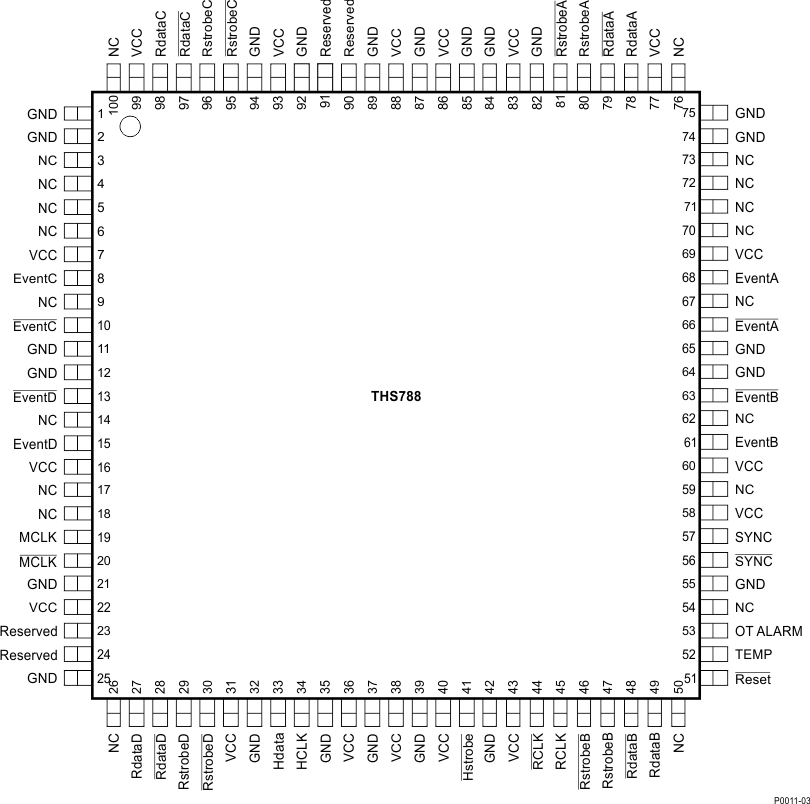
6 Pin Configuration and Functions
PFD Package
100-Pin HTQFP
(Top View)

NOTE:
Pin 1 indicator is symbolized with a white dot, and is located near pin 1 corner.Pin Functions
| PIN | TYPE | DESCRIPTION | |
|---|---|---|---|
| NAME | NO. | ||
| EventA | 68 | LVDS-compatible input | Positive event input for channel A |
| EventA | 66 | LVDS-compatible input | Negative event input for channel A |
| EventB | 61 | LVDS-compatible input | Positive event input for channel B |
| EventB | 63 | LVDS-compatible input | Negative event input for channel B |
| EventC | 8 | LVDS-compatible input | Positive event input for channel C |
| EventC | 10 | LVDS-compatible input | Negative event input for channel C |
| EventD | 15 | LVDS-compatible input | Positive event input for channel D |
| EventD | 13 | LVDS-compatible input | Negative event input for channel D |
| GND | 1, 2, 11, 12, 21, 25, 32, 35, 37, 39, 42, 55, 64, 65, 74, 75, 82, 84, 85, 87, 89, 92, 94 | Ground | Chip ground |
| HCLK | 34 | LVCMOS input | Host serial-interface clock |
| Hdata | 33 | LVCMOS I/O | Host serial-interface data I/O |
| Hstrobe | 41 | LVCMOS input | Host serial-interface chip select |
| MCLK | 19 | LVDS-compatible input | Positive master-clock input |
| MCLK | 20 | LVDS-compatible input | Negative master-clock input |
| NC | 3–6, 9, 14, 17, 18, 26, 50, 54, 59, 62, 67, 70–73, 76, 100 | No connect | Physically not connected to silicon |
| OT_ALARM | 53 | Open-drain output | Overtemperature alarm |
| RCLK | 45 | LVDS-compatible output | Positive result-interface clock |
| RCLK | 44 | LVDS-compatible output | Negative result-interface clock |
| RdataA | 78 | LVDS-compatible output | Positive result-data output for channel A |
| RdataA | 79 | LVDS-compatible output | Negative result-data output for channel A |
| RdataB | 49 | LVDS-compatible output | Positive result-data output for channel B |
| RdataB | 48 | LVDS-compatible output | Negative result-data output for channel B |
| RdataC | 98 | LVDS-compatible output | Positive result-data output for channel C |
| RdataC | 97 | LVDS-compatible output | Negative result-data output for channel C |
| RdataD | 27 | LVDS-compatible output | Positive result-data output for channel D |
| RdataD | 28 | LVDS-compatible output | Negative result-data output for channel D |
| Reserved | 23, 24, 90, 91 | Engineering or test pins | Connect to VCC |
| Reset | 51 | LVCMOS input | Chip reset, active-low |
| RstrobeA | 80 | LVDS-compatible output | Positive strobe signal for channel A |
| RstrobeA | 81 | LVDS-compatible output | Negative strobe signal for channel A |
| RstrobeB | 47 | LVDS-compatible output | Positive strobe signal for channel B |
| RstrobeB | 46 | LVDS-compatible output | Negative strobe signal for channel B |
| RstrobeC | 96 | LVDS-compatible output | Positive strobe signal for channel C |
| RstrobeC | 95 | LVDS-compatible output | Negative strobe signal for channel C |
| RstrobeD | 29 | LVDS-compatible output | Positive strobe signal for channel D |
| RstrobeD | 30 | LVDS-compatible output | Negative strobe signal for channel D |
| SYNC | 57 | LVDS-compatible input | Positive input for sync channel |
| SYNC | 56 | LVDS-compatible input | Negative input for sync channel |
| TEMP | 52 | Analog output | Die temperature |
| VCC | 7, 16, 22, 31, 36, 38, 40, 43, 58, 60, 69, 77, 83, 86, 88, 93, 99 | Power supply | Positive supply, nominal 3.3 V |