SBOS431A May 2009 – March 2017 THS6214
PRODUCTION DATA.
- 1 Features
- 2 Applications
- 3 Description
- 4 Revision History
- 5 Pin Configuration and Functions
-
6 Specifications
- 6.1 Absolute Maximum Ratings
- 6.2 ESD Ratings
- 6.3 Recommended Operating Conditions
- 6.4 Thermal Information
- 6.5 Electrical Characteristics: VS = ±12 V
- 6.6 Electrical Characteristics: VS = ±6 V
- 6.7 Timing Requirements
- 6.8 Typical Characteristics: VS = ±12 V, Full Bias
- 6.9 Typical Characteristics: VS = ±12 V, Mid Bias
- 6.10 Typical Characteristics: VS = ±12 V, Low Bias
- 6.11 Typical Characteristics: VS = ±6 V, Full Bias
- 6.12 Typical Characteristics: VS = ±6 V, Mid Bias
- 6.13 Typical Characteristics: VS = ±6 V, Low Bias
- 7 Detailed Description
- 8 Application and Implementation
- 9 Power Supply Recommendations
- 10Layout
- 11Device and Documentation Support
- 12Mechanical, Packaging, and Orderable Information
封装选项
机械数据 (封装 | 引脚)
散热焊盘机械数据 (封装 | 引脚)
- PWP|24
订购信息
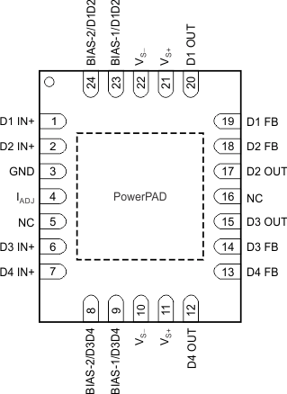
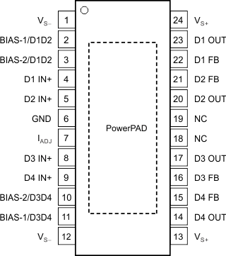
5 Pin Configuration and Functions
1. The PowerPAD is electrically isolated from all other pins and can be connected to any potential voltage range from VS– to VS+. Typically, the PowerPAD is connected to the GND plane because this plane tends to physically be the largest and is able to dissipate the most amount of heat.
2. The THS6214 defaults to the shutdown (disable) state if no signal is present on the bias pins.
3. The GND pin range is from VS– to (VS+ – 5 V).
NOTE:
NC = no connection.Pin Functions(1)
| PIN | I/O | DESCRIPTION | ||
|---|---|---|---|---|
| NAME | NO. | |||
| RHF | PWP | |||
| BIAS-1/D1D2 | 23 | 2 | I | Bias mode parallel control for port A, LSB |
| BIAS-1/D3D4 | 9 | 11 | I | Bias mode parallel control for port B, LSB |
| BIAS-2/D1D2 | 24 | 3 | I | Bias mode parallel control for port A, MSB |
| BIAS-2/D3D4 | 8 | 10 | I | Bias mode parallel control for port B, MSB |
| D1 FB | 19 | 22 | I | Amplifier D1 inverting input |
| D2 FB | 18 | 21 | I | Amplifier D2 inverting input |
| D3 FB | 14 | 16 | I | Amplifier D3 inverting input |
| D4 FB | 13 | 15 | I | Amplifier D4 inverting input |
| D1 IN+ | 1 | 4 | I | Amplifier D1 noninverting input |
| D2 IN+ | 2 | 5 | I | Amplifier D2 noninverting input |
| D3 IN+ | 6 | 8 | I | Amplifier D3 noninverting input |
| D4 IN+ | 7 | 9 | I | Amplifier D4 noninverting input |
| D1 OUT | 20 | 23 | O | Amplifier D1 output |
| D2 OUT | 17 | 20 | O | Amplifier D2 output |
| D3 OUT | 15 | 17 | O | Amplifier D3 output |
| D4 OUT | 12 | 14 | O | Amplifier D4 output |
| GND(2) | 3 | 6 | I/O | Control pin ground reference |
| IADJ | 4 | 7 | I/O | Bias current adjustment pin |
| NC | 5, 16 | 18, 19 | — | No internal connection |
| VS– | 10, 22 | 1, 12 | I/O | Negative power-supply connection |
| VS+ | 11, 21 | 11, 24 | I/O | Positive power-supply connection |
(1) The THS6214 defaults to the shutdown (disable) state if no signal is present on the bias pins.
(2) The GND pin range is from VS– to (VS+ – 5 V).
Table 1. BIAS-1, BIAS-2 Logic Table
| BIAS-1 | BIAS-0 | FUNCTION | DESCRITPION |
|---|---|---|---|
| 0 | 0 | Full bias mode (100%) | Amplifiers on with lowest distortion possible (default state) |
| 1 | 0 | Mid bias mode (75%) | Amplifiers on with power savings and a reduction in distortion performance |
| 0 | 1 | Low bias mode (50%) | Amplifiers on with enhanced power savings and a reduction of overall performance |
| 1 | 1 | Shutdown mode | Amplifiers off and output has high impedance |

