SLOS454I January 2005 – July 2016 THS4509
PRODUCTION DATA.
- 1 Features
- 2 Applications
- 3 Description
- 4 Revision History
- 5 Device Comparison Table
- 6 Pin Configuration and Functions
- 7 Specifications
- 8 Detailed Description
- 9 Application and Implementation
- 10Power Supply Recommendations
- 11Layout
- 12Device and Documentation Support
- 13Mechanical, Packaging, and Orderable Information
9 Application and Implementation
NOTE
Information in the following applications sections is not part of the TI component specification, and TI does not warrant its accuracy or completeness. TI’s customers are responsible for determining suitability of components for their purposes. Customers should validate and test their design implementation to confirm system functionality.
9.1 Application Information
The THS4509 is a fully-configurable, differential operational amplifier. The closed-loop gain is set by external resistors. Many performance metrics are set by the matching of these external resistors, so 0.1% or better tolerance resistors are recommended.
The amplifier output common-mode voltage is set by the CM pin. From the CM pin to the amplifier outputs there is a fixed gain of 1 V/V so that the amplifier output voltage is identical to the voltage applied to the CM pin. This pin must be driven by a low impedance reference and must also be bypassed to ground using a 0.1-µF ceramic, low ESR resistor. The ideal common-mode voltage is equal to the voltage that is midway between the positive and negative supply voltages.
The THS4509 can be operated from either single or split power supplies with a range of 3 V to 5 V of total supply voltage. When selecting a power supply voltage, make sure to provide adequate margin for input and output voltage levels. In many cases, split supplies are the best option. It is not necessary to have power supply voltages symmetrical around ground. For example, –1 V and +4 V is a valid power supply configuration.
9.2 Typical Applications
The following circuits show application information for the THS4509. For simplicity, power-supply decoupling capacitors are not shown in these diagrams. See the Layout section for recommendations. For more detail on the use and operation of fully-differential op amps refer to the application report, Fully-Differential Amplifiers (SLOA054).
9.2.1 Differential Input to Differential Output Amplifier
The THS4509 is a fully-differential op amp, and can be used to amplify differential input signals to differential output signals. A basic block diagram of the circuit is shown in Figure 81 (CM input not shown). The gain of the circuit is set by RF divided by RG.
Depending on the source and load, input and output termination can be accomplished by adding RIT and RO.
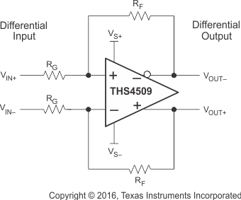 Figure 81. Differential Input to Differential-Output Amplifier
9.2.1.1 Design Requirements
The following sections detail how to determine if your design meets these requirements.
The main design requirements for the THS4509 are the input common mode, the output swing voltage. Other design requirements are signal linearity and accuracy. With flexible supply voltage ranges and externally configurable resistors the THS4509 can be configured to meet many design requirements.
Table 5 lists the design parameters of this example.
Table 5. Design Parameters
| PARAMETER | EXAMPLE VALUE |
|---|---|
| Gain | 6 dB |
| Output swing | 2 Vpp |
| Harmonic distortion | >75 dBc |
| Load resistance | 100 Ω |
9.2.1.2 Detailed Design Procedure
The first parameter is gain. Gain is set by external resistors as shown in Table 3. With a gain of 6 dB, the appropriate resistor values are 348 Ω for RF and 165 Ω for RG and 61.9 Ω for the termination resistor. These resistor values are for a 50-Ω source. The desired output swing of 2 Vpp and distortion of –75 dBc means that a supply voltage of 5 V is required. Further design details are covered in this section.
9.2.1.2.1 Input Common-Mode Voltage Range
The input common-mode voltage of a fully-differential op amp is the voltage at the + and – input pins of the op amp.
It is important to not violate the input common-mode voltage range (VICR) of the op amp. Assuming the op amp is in linear operation the voltage across the input pins is only a few millivolts at most. So finding the voltage at one input pin determines the input common-mode voltage of the op amp.
Treating the negative input as a summing node, the voltage is given by Equation 1:

To determine the VICR of the op amp, the voltage at the negative input is evaluated at the extremes of VOUT+.
As the gain of the op amp increases, the input common-mode voltage becomes closer and closer to the input common-mode voltage of the source.
9.2.1.2.2 Setting the Output Common-Mode Voltage
The output common-mode voltage is set by the voltage at the CM pin(s). The internal common-mode control circuit maintains the output common-mode voltage within 3-mV offset (typical) from the set voltage, when set within 0.5 V of midsupply, with less than 4-mV differential offset voltage. If left unconnected, the common-mode set point is set to midsupply by internal circuitry, which may be overdriven from an external source. Figure 82 is representative of the CM input. The internal CM circuit has about 700 MHz of –3-dB bandwidth, which is required for best performance, but it is intended to be a DC bias input pin. Bypass capacitors are recommended on this pin to reduce noise at the output. The external current required to overdrive the internal resistor divider is given by Equation 2:

where
- VCM is the voltage applied to the CM pin
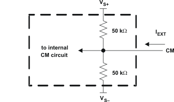 Figure 82. CM Input Circuit
9.2.1.2.3 Single-Supply Operation (3 V to 5 V)
To facilitate testing with common lab equipment, the THS4509 EVM allows split-supply operation, and the characterization data presented in this data sheet were taken with split-supply power inputs. The device can easily be used with a single-supply power input without degrading the performance. Figure 83, Figure 84, and Figure 85 show DC and AC-coupled single-supply circuits with single-ended inputs. These configurations all allow the input and output common-mode voltage to be set to midsupply allowing for optimum performance. The information presented here can also be applied to differential input sources.
In Figure 83, the source is referenced to the same voltage as the CM pin (VCM). VCM is set by the internal circuit to midsupply. RT along with the input impedance of the amplifier circuit provides input termination, which is also referenced to VCM.
NOTE
RS and RT are added to the alternate input from the signal input to balance the amplifier. Alternately, one resistor can be used equal to the combined value RG+ RS || RT on this input. This is also true of the circuits shown in Figure 84 and Figure 85.
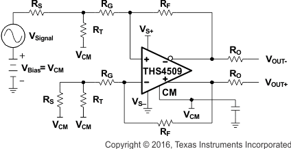 Figure 83. THS4509 DC-Coupled Single-Supply With Input Biased to VCM
In Figure 84 the source is referenced to ground and so is the input termination resistor. RPU is added to the circuit to avoid violating the VICR of the op amp. The proper value of resistor to add can be calculated from Equation 3:

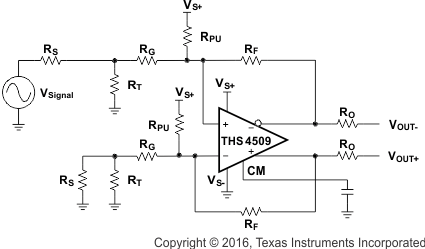 Figure 84. THS4509 DC-Coupled Single-Supply With RPU Used to Set VIC
VIC is the desired input common-mode voltage, VCM = CM, and RIN = RG+ RS || RT. To set to midsupply, make the value of RPU = RG+ RS || RT.
Table 6 is a modification of Table 3 to add the proper values with RPU assuming a 50-Ω source impedance and setting the input and output common-mode voltage to midsupply.
Table 6. RPU Values for Various Gains
| GAIN | RF | RG | RIT | RPU |
|---|---|---|---|---|
| 6 dB | 348 Ω | 169 Ω | 64.9 Ω | 200 Ω |
| 10 dB | 348 Ω | 102 Ω | 78.7 Ω | 133 Ω |
| 14 dB | 348 Ω | 61.9 Ω | 115 Ω | 97.6 Ω |
| 20 dB | 348 Ω | 40.2 Ω | 221 Ω | 80.6 Ω |
There are two drawbacks to this configuration. One is that it requires additional current from the power supply. Using the values shown for a gain of 10 dB requires 37 mA more current with 5-V supply, and 22-mA more current with 3-V supply.
The other drawback is that this configuration also increases the noise gain of the circuit. In the 10-dB gain case, noise gain increases by a factor of 1.5.
Figure 85 shows AC coupling to the source. Using capacitors in series with the termination resistors allows the amplifier to self-bias both input and output to midsupply.
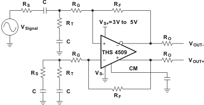 Figure 85. THS4509 AC-Coupled Single-Supply
9.2.1.2.4 THS4509 and ADS5500 Combined Performance
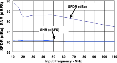
The THS4509 is designed to be a high-performance drive amplifier for high-performance data converters like the ADS5500 14-bit 125-MSPS ADC. Figure 86 shows a circuit combining the two devices, and Figure 87 shows the combined SNR and SFDR performance versus frequency with –1-dBFS input signal level sampling at 125 MSPS. The THS4509 amplifier circuit provides 10 dB of gain, converts the single-ended input to differential, and sets the proper input common-mode voltage to the ADS5500. The 100-Ω resistors and 2.7-pF capacitor between the THS4509 outputs and ADS5500 inputs along with the input capacitance of the ADS5500 limit the bandwidth of the signal to 115 MHz (–3 dB). For testing, a signal generator is used for the signal source. The generator is an ac-coupled 50-Ω source. A band-pass filter is inserted in series with the input to reduce harmonics and noise from the signal source. Input termination is accomplished through the 69.8-Ω resistor and 0.22-μF capacitor to ground in conjunction with the input impedance of the amplifier circuit. A 0.22-μF capacitor and 49.9-Ω resistor is inserted to ground across the 69.8-Ω resistor and 0.22-μF capacitor on the alternate input to balance the circuit. Gain is a function of the source impedance, termination, and 348-Ω feedback resistor. Refer to Table 6 for component values to set proper 50-Ω termination for other common gains. A split power supply of +4 V and –1 V is used to set the input and output common-mode voltages to approximately midsupply while setting the input common-mode of the ADS5500 to the recommended +1.55 V. This configuration maintains maximum headroom on the internal transistors of the THS4509 to insure optimum performance.
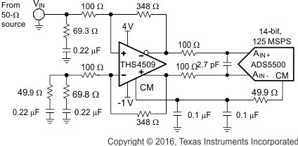 Figure 86. THS4509 and ADS5500 Circuit
Figure 88 shows the two-tone FFT of the THS4509 and ADS5500 circuit with 65-MHz and 70-MHz input frequencies. The SFDR is 90 dBc.
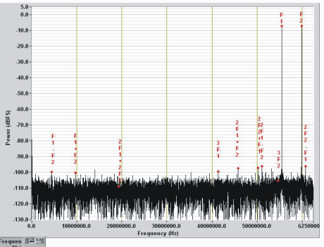 Figure 88. THS4509 and ADS5500 2-Tone FFT With 65-MHz and 70-MHz Inputs
9.2.1.2.5 THS4509 and ADS5424 Combined Performance
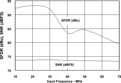
Figure 89 shows the THS4509 driving the ADS5424 ADC, and Figure 90 shows the combined SNR and SFDR performance versus frequency with –1-dBFS input signal level and sampling at 80 MSPS.
As before, the THS4509 amplifier provides 10 dB of gain, converts the single-ended input to differential, and sets the proper input common-mode voltage to the ADS5424. Input termination and circuit testing is the same as described above for the THS4509 and ADS5500 circuit.
The 225-Ω resistors and 2.7-pF capacitor between the THS4509 outputs and ADS5424 inputs (along with the input capacitance of the ADC) limit the bandwidth of the signal to about 100MHz (–3 dB).
Because the ADS5424 recommended input common-mode voltage is 2.4 V, the THS4509 is operated from a single power-supply input with VS+ = 5 V and VS– = 0 V (ground).
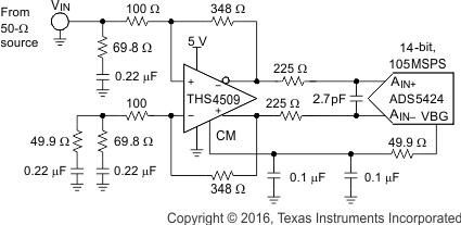 Figure 89. THS4509 and ADS5424 Circuit
9.2.2 Single-Ended Input to Differential Output Amplifier
The THS4509 can be used to amplify and convert single-ended input signals to differential output signals. A basic block diagram of the circuit is shown in Figure 91 (CM input not shown). The gain of the circuit is again set by RF divided by RG.
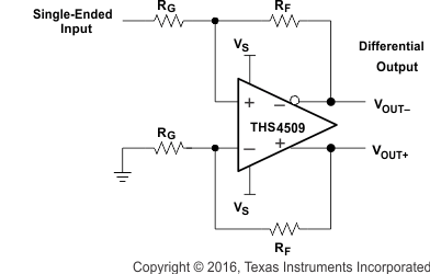 Figure 91. Single-Ended Input to Differential Output Amplifier
