ZHCSPA5F August 1999 – July 2024 THS4021 , THS4022
PRODUCTION DATA
- 1
- 1 特性
- 2 应用
- 3 说明
- 4 Pin Configuration and Functions
-
5 Specifications
- 5.1 Absolute Maximum Ratings
- 5.2 ESD Ratings
- 5.3 Recommended Operating Conditions
- 5.4 Thermal Information - THS4021
- 5.5 Thermal Information - THS4022
- 5.6 Electrical Characteristics - THS4021D and THS4022DGN
- 5.7 Electrical Characteristics - THS4021DGN
- 5.8 Typical Characteristics: THS4021D and THS4022DGN
- 5.9 Typical Characteristics: THS4021DGN
- 6 Detailed Description
- 7 Application and Implementation
- 8 Device and Documentation Support
- 9 Revision History
- 10Mechanical, Packaging, and Orderable Information
封装选项
请参考 PDF 数据表获取器件具体的封装图。
机械数据 (封装 | 引脚)
- D|8
- DGN|8
散热焊盘机械数据 (封装 | 引脚)
- DGN|8
订购信息
4 Pin Configuration and Functions
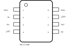 Figure 4-1 THS4021: D Package, 8-Pin SOIC, or DGN Package, 8-pin HVSSOP (Top
View)
Figure 4-1 THS4021: D Package, 8-Pin SOIC, or DGN Package, 8-pin HVSSOP (Top
View)Table 4-1 Pin Functions: THS4021
| PIN | TYPE | DESCRIPTION | |
|---|---|---|---|
| NAME | NO. | ||
| IN– | 2 | Input | Inverting input |
| IN+ | 3 | Input | Noninverting input |
| NC | 5 | — | No connection |
| NULL | 1, 8 | Input | Voltage offset adjust |
| OUT | 6 | Output | Output of amplifier |
| VCC– | 4 | — | Negative power supply |
| VCC+ | 7 | — | Positive power supply |
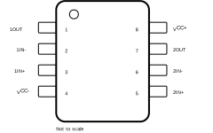 Figure 4-2 THS4022: DGN Package, 8-pin HVSSOP (Top View)
Table 4-2 Pin Functions: THS4022
| PIN | TYPE | DESCRIPTION | |
|---|---|---|---|
| NAME | NO. | ||
| 1IN– | 2 | Input | Channel 1 inverting input |
| 1IN+ | 3 | Input | Channel 1 noninverting input |
| 1OUT | 1 | Output | Channel 1 output |
| 2IN– | 6 | Input | Channel 2 inverting input |
| 2IN+ | 5 | Input | Channel 2 noninverting input |
| 2OUT | 7 | Output | Channel 2 output |
| VCC– | 4 | — | Negative power supply |
| VCC+ | 8 | — | Positive power supply |