ZHCSFY1F December 2016 – April 2024 TDP158
PRODUCTION DATA
- 1
- 1 特性
- 2 应用
- 3 说明
- 4 Pin Configuration and Functions
-
5 Specifications
- 5.1 Absolute Maximum Ratings
- 5.2 ESD Ratings
- 5.3 Recommended Operating Conditions
- 5.4 Thermal Information
- 5.5 Electrical Characteristics, Power Supply
- 5.6 Electrical Characteristics, Differential Input
- 5.7 Electrical Characteristics, TMDS Differential Output
- 5.8 Electrical Characteristics, DDC, I2C, HPD, and ARC
- 5.9 Electrical Characteristics, TMDS Differential Output in DP-Mode
- 5.10 Switching Characteristics, TMDS
- 5.11 Switching Characteristics, HPD
- 5.12 Switching Characteristics, DDC and I2C
- 5.13 Typical Characteristics
- 6 Parameter Measurement Information
-
7 Detailed Description
- 7.1 Overview
- 7.2 Functional Block Diagram
- 7.3 Feature Description
- 7.4 Device Functional Modes
- 7.5
Register Maps
- 7.5.1 Local I2C Control BIT Access TAG Convention
- 7.5.2 BIT Access Tag Conventions
- 7.5.3 CSR Bit Field Definitions, DEVICE_ID (address = 00h≅07h)
- 7.5.4 CSR Bit Field Definitions, REV_ID (address = 08h )
- 7.5.5 CSR Bit Field Definitions – MISC CONTROL 09h (address = 09h)
- 7.5.6 CSR Bit Field Definitions – MISC CONTROL 0Ah (address = 0Ah)
- 7.5.7 CSR Bit Field Definitions – MISC CONTROL 0Bh (address = 0Bh)
- 7.5.8 CSR Bit Field Definitions – MISC CONTROL 0Ch (address = 0Ch)
- 7.5.9 CSR Bit Field Definitions, Equalization Control Register (address = 0Dh)
- 7.5.10 CSR Bit Field Definitions, POWER MODE STATUS (address = 20h)
- 7.5.11 CSR Bit Field Definitions, DP-Mode and INDIVIDUAL LANE CONTROL (address = 30h)
- 7.5.12 CSR Bit Field Definitions, DP-Mode and INDIVIDUAL LANE CONTROL (address = 31h)
- 7.5.13 CSR Bit Field Definitions, DP-Mode and INDIVIDUAL LANE CONTROL (address = 32h)
- 7.5.14 CSR Bit Field Definitions, DP-Mode and INDIVIDUAL LANE CONTROL (address = 33h)
- 7.5.15 CSR Bit Field Definitions, DP-Mode and INDIVIDUAL LANE CONTROL (address = 34h)
- 7.5.16 CSR Bit Field Definitions, DP-Mode and INDIVIDUAL LANE CONTROL (address = 35h)
- 7.5.17 CSR Bit Field Definitions, DP-Mode and INDIVIDUAL LANE CONTROL (address = 4Dh)
- 7.5.18 CSR Bit Field Definitions, DP-Mode and INDIVIDUAL LANE CONTROL (address = 4Eh)
- 7.5.19 CSR Bit Field Definitions, DP-Mode and INDIVIDUAL LANE CONTROL (address = 4Fh)
- 8 Application and Implementation
- 9 Device and Documentation Support
- 10Revision History
- 11Mechanical, Packaging, and Orderable Information
6 Parameter Measurement Information
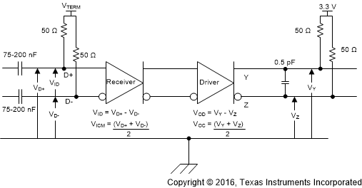 Figure 6-1 TMDS Main Link Test Circuit
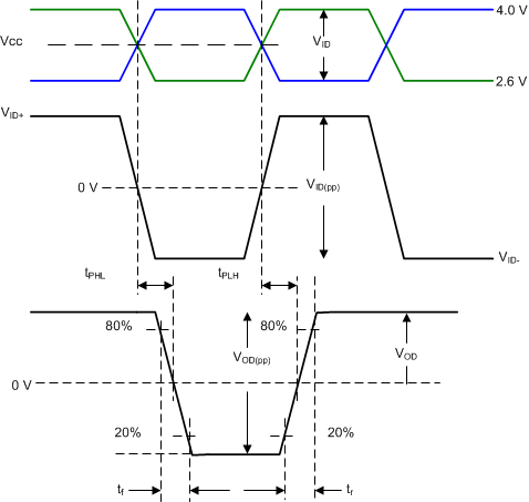 Figure 6-2 Input or Output Timing Measurements
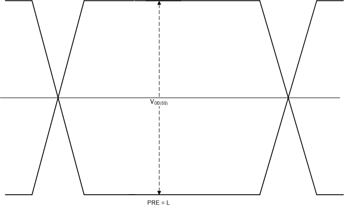 Figure 6-3 Output Differential Waveform
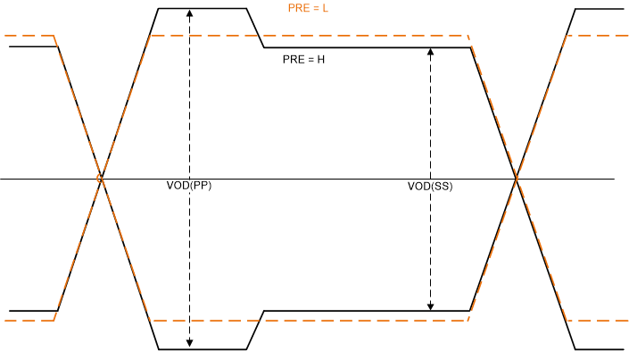 Figure 6-4 Output Differential Waveform with
De-Emphasis
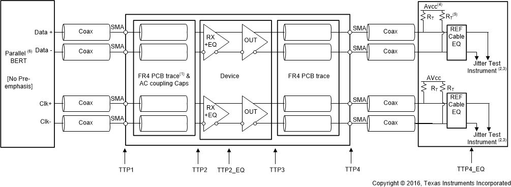
A. The FR4 trace between TTP1 and TTP2 is designed to emulate 1-8” of FR4, AC coupling
capacitor, connector and another 1-8” of FR4. Trace width – 4 mils. 100Ω differential
impedance.
B. All Jitter is measured at a BER of
109
C. Residual jitter reflects the total jitter
measured at TTP4 minus the jitter measured at
TTP
D. AVCC = 3.3V
E. RT = 50Ω
F. The input signal from parallel Bert does not have
any pre-emphasis. Refer to Recommended
Operating Conditions.
Figure 6-5 HDMI Output Jitter Measurement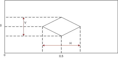 Figure 6-6 Output Eye Mask at TTP4_EQ for HDMI 2.0
| TMDS Data Rate (Gbps) | H (Tbit) | V (mV) |
|---|---|---|
| 3.4 < DR < 3.712 | 0.6 | 335 |
| 3.712 < DR < 5.94 | –0.0332Rbit2 + 0.2312 Rbit + 0.1998 | –19.66Rbit2 + 106.74Rbit + 209.58 |
| 5.94 ≤ DR ≤ 6.0 | 0.4 | 150 |
 Figure 6-7 HPD Test Circuit
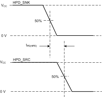 Figure 6-8 HPD
Timing Diagram No. 1
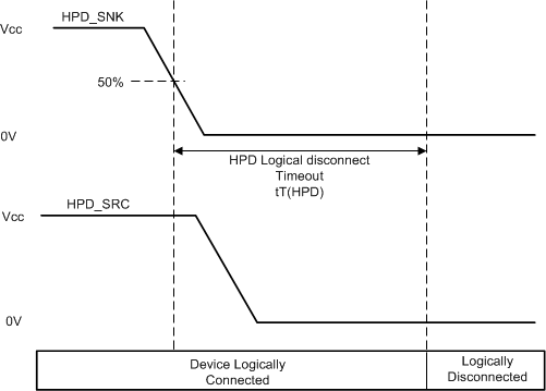 Figure 6-9 HPD
Logic Disconnect Timeout
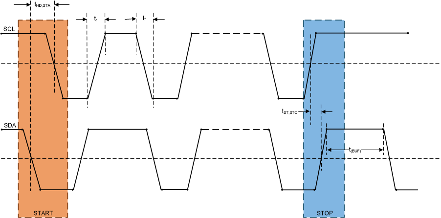 Figure 6-10 Start and Stop Condition Timing
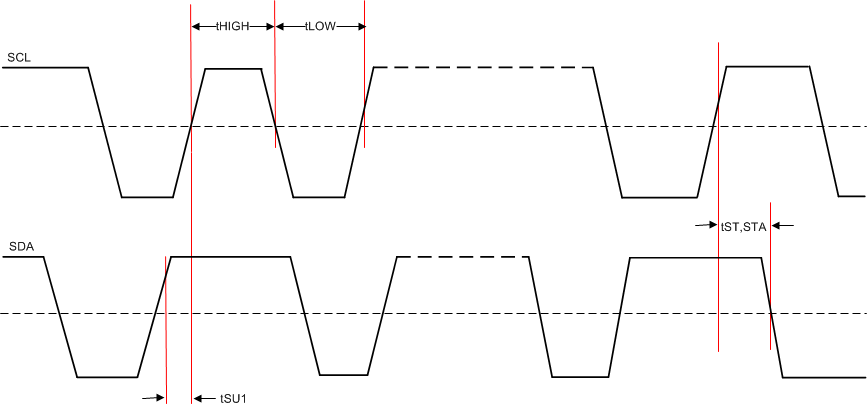 Figure 6-11 SCL
and SDA Timing
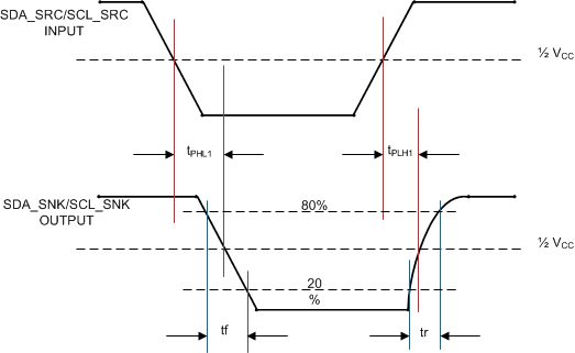 Figure 6-12 DDC
Propagation Delay – Source to Sink
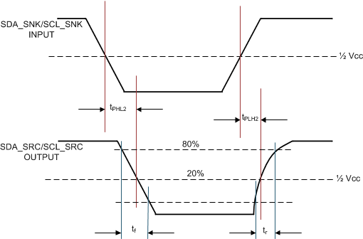 Figure 6-13 DDC
Propagation Delay – Sink to Source
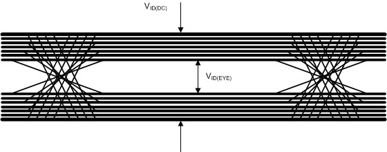 Figure 6-14 VID(DC) and
VID(EYE)