ZHCSC52D January   2014  – November 2019 TCA9545A

PRODUCTION DATA.  

  1. 特性
  2. 应用
  3. 说明
    1.     Device Images
      1.      简化的应用示意图
  4. 修订历史记录
  5. Pin Configuration and Functions
    1.     Pin Functions
  6. Specifications
    1. 6.1 Absolute Maximum Ratings
    2. 6.2 ESD Ratings
    3. 6.3 Recommended Operating Conditions
    4. 6.4 Thermal Information
    5. 6.5 Electrical Characteristics
    6. 6.6 I2C Interface Timing Requirements
    7. 6.7 Switching Characteristics
    8. 6.8 Interrupt and Reset Timing Requirements
    9. 6.9 Typical Characteristics
  7. Parameter Measurement Information
  8. Detailed Description
    1. 8.1 Overview
    2. 8.2 Functional Block Diagram
    3. 8.3 Feature Description
    4. 8.4 Device Functional Modes
      1. 8.4.1 RESET Input
      2. 8.4.2 Power-On Reset
    5. 8.5 Programming
      1. 8.5.1 I2C Interface
    6. 8.6 Control Register
      1. 8.6.1 Device Address
      2. 8.6.2 Control Register Description
      3. 8.6.3 Control Register Definition
      4. 8.6.4 Interrupt Handling
  9. Application and Implementation
    1. 9.1 Application Information
    2. 9.2 Typical Application
      1. 9.2.1 Design Requirements
      2. 9.2.2 Detailed Design Procedure
      3. 9.2.3 TCA9545A Application Curves
  10. 10Power Supply Recommendations
    1. 10.1 Power-On Reset Requirements
  11. 11Layout
    1. 11.1 Layout Guidelines
    2. 11.2 Layout Example
  12. 12器件和文档支持
    1. 12.1 接收文档更新通知
    2. 12.2 支持资源
    3. 12.3 商标
    4. 12.4 静电放电警告
    5. 12.5 Glossary
  13. 13机械、封装和可订购信息

封装选项

机械数据 (封装 | 引脚)
散热焊盘机械数据 (封装 | 引脚)
订购信息

Control Register Description

Following the successful acknowledgment of the slave address, the bus master sends a byte to the TCA9545A, which is stored in the control register (see Figure 15). If multiple bytes are received by the TCA9545A, it saves the last byte received. This register can be written and read via the I2C bus.
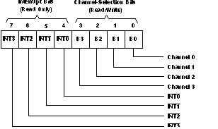
TCA9545A cont_reg_cps204.gifFigure 15. Control Register