ZHCSIF1A June   2018  – February 2022 TCA9517-Q1

PRODUCTION DATA  

  1. 特性
  2. 应用
  3. 说明
  4. Revision History
  5. 说明(续)
  6. Pin Configuration and Functions
  7. Specifications
    1. 7.1 Absolute Maximum Ratings
    2. 7.2 ESD Ratings
    3. 7.3 Recommended Operating Conditions
    4. 7.4 Thermal Information
    5. 7.5 Electrical Characteristics
    6. 7.6 Timing Requirements
    7. 7.7 I2C Interface Switching Characteristics
    8. 7.8 Typical Characteristics
  8. Parameter Measurement Information
  9. Detailed Description
    1. 9.1 Overview
    2. 9.2 Functional Block Diagram
    3. 9.3 Feature Description
      1. 9.3.1 Two-Channel Bidirectional Buffer
      2. 9.3.2 Active-High Repeater-Enable Input
      3. 9.3.3 VOL B-Side Offset Voltage
      4. 9.3.4 Standard Mode and Fast Mode Support
      5. 9.3.5 Clock Stretching Support
    4. 9.4 Device Functional Modes
  10. 10Application and Implementation
    1. 10.1 Application Information
    2. 10.2 Typical Application
      1. 10.2.1 Design Requirements
      2. 10.2.2 Detailed Design Procedure
        1. 10.2.2.1 Clock Stretching Support
        2. 10.2.2.2 VILC and Pullup Resistor Sizing
      3. 10.2.3 Application Curve
  11. 11Power Supply Recommendations
  12. 12Layout
    1. 12.1 Layout Guidelines
    2. 12.2 Layout Example
  13. 13Device and Documentation Support
    1. 13.1 Device Support
    2. 13.2 Receiving Notification of Documentation Updates
    3. 13.3 支持资源
    4. 13.4 Trademarks
    5. 13.5 Electrostatic Discharge Caution
    6. 13.6 术语表

封装选项

机械数据 (封装 | 引脚)
散热焊盘机械数据 (封装 | 引脚)
订购信息

Layout Example

Figure 12-1 shows an example layout of the DGK package.
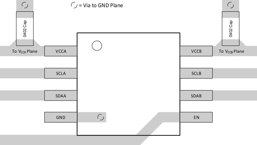
GUID-12458F80-ADE3-4BE4-97DD-0357D16015C9-low.gifFigure 12-1 TCA9517-Q1A Layout Example