SCPS164D MAY 2007 – February 2017 TCA6507
PRODUCTION DATA.
- 1 Features
- 2 Applications
- 3 Description
- 4 Revision History
- 5 Pin Configuration and Functions
- 6 Specifications
- 7 Parameter Measurement Information
-
8 Detailed Description
- 8.1 Overview
- 8.2 Functional Block Diagram
- 8.3 Feature Description
- 8.4 Device Functional Modes
- 8.5 Programming
- 8.6
Register Maps
- 8.6.1 Registers 0x00 - 0x02 (Select Registers)
- 8.6.2 Register 0x03 (Fade-ON Time)
- 8.6.3 Register 0x04 (Fully-ON Time)
- 8.6.4 Register 0x05 (Fade-OFF Time)
- 8.6.5 Register 0x06 - 0x07 (Fully-OFF Time)
- 8.6.6 Register 0x08 (Maximum Intensity per Bank)
- 8.6.7 Register 0x09 (One-Shot / Master Intensity)
- 8.6.8 Register 0x0A (Initialization Register)
- 9 Application and Implementation
- 10Power Supply Recommendations
- 11Layout
- 12Device and Documentation Support
- 13Mechanical, Packaging, and Orderable Information
封装选项
机械数据 (封装 | 引脚)
散热焊盘机械数据 (封装 | 引脚)
- RUE|12
订购信息
11 Layout
11.1 Layout Guidelines
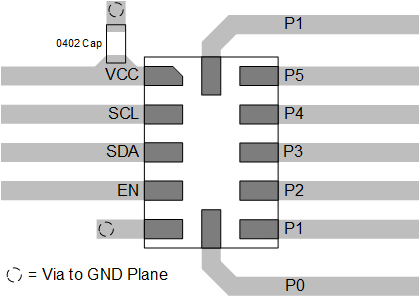
For PCB layout of the TCA6507, common PCB layout practices must be followed, but additional concerns related to high-speed data transfer, such as matched impedances and differential pairs, are not a concern for I2C signals speeds. It is common to have a dedicated ground plane on an inner layer of the board, and pins that are connected to ground must have a low-impedance path to the ground plane in the form of wide polygon pours, and multiple vias. By-pass and de-coupling capacitors are commonly used to control the voltage on the VCC pin, using a larger capacitor to provide additional power in the event of a short power supply glitch, and a smaller capacitor to filter out high-frequency ripple.
11.2 Layout Example
 Figure 28. RUE Layout Recommendation