ZHCSBA9C July 2013 – November 2017 TAS5760LD
PRODUCTION DATA.
- 1 特性
- 2 应用
- 3 说明
- 4 修订历史记录
- 5 Pin Configuration and Functions
-
6 Specifications
- 6.1 Absolute Maximum Ratings
- 6.2 ESD Ratings
- 6.3 Recommended Operating Conditions
- 6.4 Thermal Information
- 6.5 Digital I/O Pins
- 6.6 Master Clock
- 6.7 Serial Audio Port
- 6.8 Protection Circuitry
- 6.9 Speaker Amplifier in All Modes
- 6.10 Speaker Amplifier in Stereo Bridge-Tied Load (BTL) Mode
- 6.11 Speaker Amplifier in Mono Parallel Bridge-Tied Load (PBTL) Mode
- 6.12 Headphone Amplifier and Line Driver
- 6.13 I²C Control Port
- 6.14 Typical Idle, Mute, Shutdown, Operational Power Consumption
- 6.15 Typical Speaker Amplifier Performance Characteristics (Stereo BTL Mode)
- 6.16 Typical Performance Characteristics (Mono PBTL Mode)
- 7 Parameter Measurement Information
-
8 Detailed Description
- 8.1 Overview
- 8.2 Functional Block Diagram
- 8.3 Feature Description
- 8.4
Device Functional Modes
- 8.4.1
Hardware Control Mode
- 8.4.1.1 Speaker Amplifier Shut Down (SPK_SD Pin)
- 8.4.1.2 Serial Audio Port in Hardware Control Mode
- 8.4.1.3 Soft Clipper Control (SFT_CLIP Pin)
- 8.4.1.4 Speaker Amplifier Switching Frequency Select (FREQ/SDA Pin)
- 8.4.1.5 Parallel Bridge Tied Load Mode Select (PBTL/SCL Pin)
- 8.4.1.6 Speaker Amplifier Sleep Enable (SPK_SLEEP/ADR Pin)
- 8.4.1.7 Speaker Amplifier Gain Select (SPK_GAIN [1:0] Pins)
- 8.4.1.8 Considerations for Setting the Speaker Amplifier Gain Structure
- 8.4.2 Software Control Mode
- 8.4.1
Hardware Control Mode
- 8.5
Register Maps
- 8.5.1 Control Port Registers - Quick Reference
- 8.5.2
Control Port Registers - Detailed Description
- 8.5.2.1 Device Identification Register (0x00)
- 8.5.2.2 Power Control Register (0x01)
- 8.5.2.3 Digital Control Register (0x02)
- 8.5.2.4 Volume Control Configuration Register (0x03)
- 8.5.2.5 Left Channel Volume Control Register (0x04)
- 8.5.2.6 Right Channel Volume Control Register (0x05)
- 8.5.2.7 Analog Control Register (0x06)
- 8.5.2.8 Reserved Register (0x07)
- 8.5.2.9 Fault Configuration and Error Status Register (0x08)
- 8.5.2.10 Reserved Controls (9 / 0x09) - (15 / 0x0F)
- 8.5.2.11 Digital Clipper Control 2 Register (0x10)
- 8.5.2.12 Digital Clipper Control 1 Register (0x11)
-
9 Application and Implementation
- 9.1 Application Information
- 9.2
Typical Applications
- 9.2.1
Stereo BTL Using Software Control
- 9.2.1.1 Design Requirements
- 9.2.1.2
Detailed Design Procedure
- 9.2.1.2.1 Startup Procedures- Software Control Mode
- 9.2.1.2.2 Shutdown Procedures- Software Control Mode
- 9.2.1.2.3 Component Selection and Hardware Connections
- 9.2.1.2.4 Recommended Startup and Shutdown Procedures
- 9.2.1.2.5
Headphone and Line Driver Amplifier
- 9.2.1.2.5.1 Charge-Pump Flying Capacitor and DR_VSS Capacitor
- 9.2.1.2.5.2 Decoupling Capacitors
- 9.2.1.2.5.3 Gain-Setting Resistor Ranges
- 9.2.1.2.5.4 Using the Line Driver Amplifier in the TAS5760LD as a Second-Order Filter
- 9.2.1.2.5.5 External Undervoltage Detection
- 9.2.1.2.5.6 Input-Blocking Capacitors
- 9.2.1.2.6 Gain-Setting Resistors
- 9.2.1.3 Application Curves
- 9.2.2 Stereo BTL Using Hardware Control
- 9.2.3 Mono PBTL Using Software Control
- 9.2.4 Mono PBTL Using Hardware Control
- 9.2.1
Stereo BTL Using Software Control
- 10Power Supply Recommendations
- 11Layout
- 12器件和文档支持
- 13机械、封装和可订购信息
6.15 Typical Speaker Amplifier Performance Characteristics (Stereo BTL Mode)
At TA = 25°C, fSPK_AMP = 384 kHz, input signal is 1 kHz Sine, unless otherwise noted. Filter used for 8 Ω = 22 µH + 0.68 µF, Filter used for 6 Ω = 15 µH + 0.68 µF, Filter used for 4 Ω = 10 µH + 0.68 µF unless otherwise noted.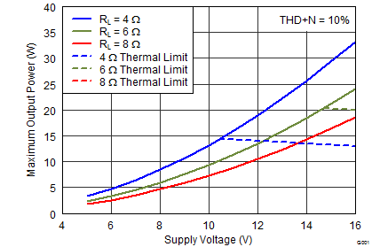
Thermal Limits are referenced to TAS5760xxEVM Rev D
Figure 1. Output Power vs PVDD
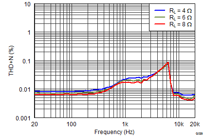
PVDD = 12 V, POSPK = 1 W
Figure 3. THD+N vs Frequency
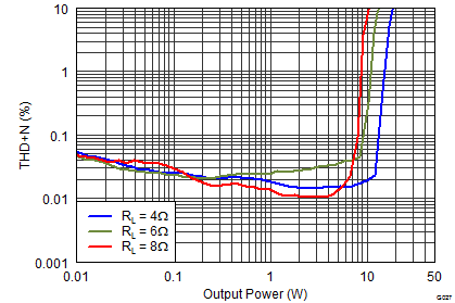
PVDD = 12 V, Both Channels Driven
Figure 5. THD+N vs Output Power
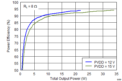 Figure 7. Efficiency vs Output Power
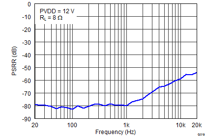 Figure 9. PVDD PSRR vs Frequency
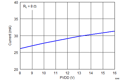 Figure 11. Idle Current Draw vs PVDD (Filterless)
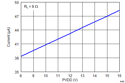 Figure 13. Shutdown Current Draw vs PVDD (Filterless)
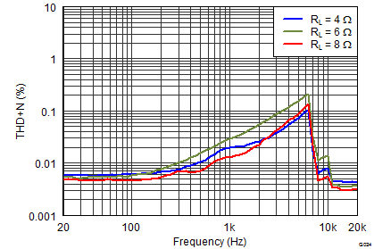
PVDD = 12 V, POSPK = 1 W
Figure 2. THD+N vs Frequency
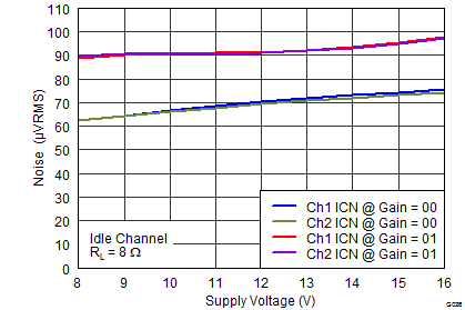 Figure 4. Idle Channel Noise vs PVDD
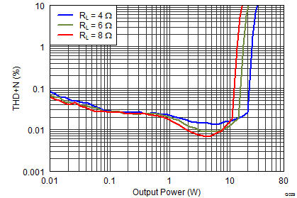
PVDD = 12 V, Both Channels Driven
Figure 6. THD+N vs Output Power
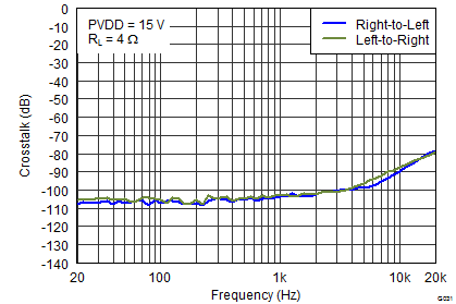 Figure 8. Crosstalk vs Frequency
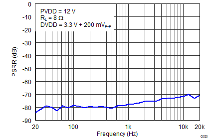 Figure 10. DVDD PSRR vs Frequency
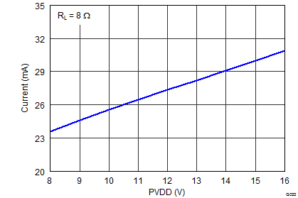
With LC Filter as shown on the EVM
Figure 12. Idle Current Draw vs PVDD
Filter used for 8 Ω = 22 µH + 0.68 µF, Filter used for 6 Ω = 15 µH + 0.68 µF, Filter used for 4 Ω = 10 µH + 0.68 µF unless otherwise noted.
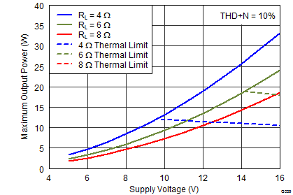
Thermal Limits are referenced to TAS5760xxEVM Rev D
Figure 14. Output Power vs PVDD
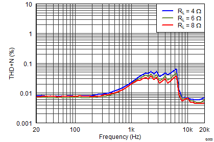
PVDD = 12 V, POSPK = 1 W
Figure 16. THD+N vs Frequency
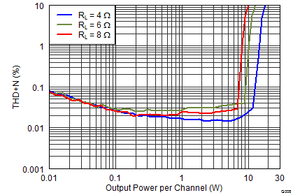
PVDD = 12 V, Both Channels Driven
Figure 18. THD+N vs Output Power
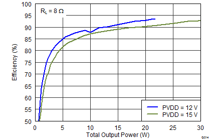 Figure 20. Efficiency vs Output Power
 Figure 22. PVDD PSRR vs Frequency
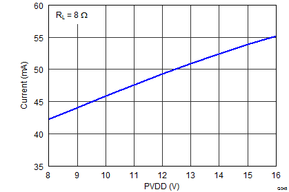 Figure 24. Idle Current Draw vs PVDD (with LC Filter as shown on EVM)
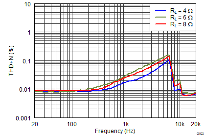
PVDD = 12 V, POSPK = 1 W
Figure 15. THD+N vs Frequency
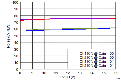 Figure 17. Idle Channel Noise vs PVDD
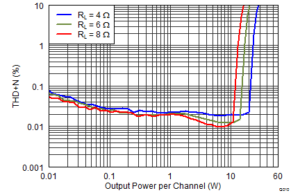
PVDD = 12 V, Both Channels Driven
Figure 19. THD+N vs Output Power
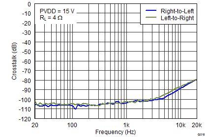 Figure 21. Crosstalk vs Frequency
 Figure 23. Idle Current Draw vs PVDD (Filterless)
 Figure 25. Shutdown Current Draw vs PVDD (Filterless)