SLES217D November 2010 – March 2015 TAS5630B
PRODUCTION DATA.
- 1 Features
- 2 Applications
- 3 Description
- 4 Revision History
- 5 Pin Configuration and Functions
- 6 Specifications
-
7 Detailed Description
- 7.1 Overview
- 7.2 Functional Block Diagram
- 7.3
Feature Description
- 7.3.1 Power Supplies
- 7.3.2 System Power-Up and Power-Down Sequence
- 7.3.3 Error Reporting
- 7.3.4 Device Protection System
- 7.3.5 Pin-to-Pin Short-Circuit Protection (PPSC)
- 7.3.6 Overtemperature Protection
- 7.3.7 Undervoltage Protection (UVP) and Power-On Reset (POR)
- 7.3.8 Device Reset
- 7.3.9 Click and Pop in SE-Mode
- 7.3.10 PBTL Overload and Short Circuit
- 7.3.11 Oscillator
- 7.4 Device Functional Modes
-
8 Application and Implementation
- 8.1 Application Information
- 8.2
Typical Application
- 8.2.1 Typical Application Schematic
- 8.2.2 Typical Differential-Input BTL Application With BD Modulation Filters
- 8.2.3 Typical Differential (2N) PBTL Application With BD Modulation Filters
- 8.2.4 Typical SE Application
- 8.2.5 Typical 2.1 System Differential-Input BTL and Unbalanced-Input SE Application
- 8.2.6 Typical Differential-Input BTL Application With BD Modulation Filters, DKD Package
- 9 Power Supply Recommendations
- 10Layout
- 11Device and Documentation Support
- 12Mechanical, Packaging, and Orderable Information
6 Specifications
6.1 Absolute Maximum Ratings
over operating free-air temperature range unless otherwise noted (1)| MIN | MAX | UNIT | ||
|---|---|---|---|---|
| VDD to AGND | –0.3 | 13.2 | V | |
| GVDD to AGND | –0.3 | 13.2 | V | |
| PVDD_X to GND_X(2) | –0.3 | 69 | V | |
| OUT_X to GND_X(2) | –0.3 | 69 | V | |
| BST_X to GND_X(2) | –0.3 | 82.2 | V | |
| BST_X to GVDD_X(2) | –0.3 | 69 | V | |
| VREG to AGND | –0.3 | 4.2 | V | |
| GND_X to GND | –0.3 | 0.3 | V | |
| GND_X to AGND | –0.3 | 0.3 | V | |
| OC_ADJ, M1, M2, M3, OSC_IO+, OSC_IO–, FREQ_ADJ, VI_CM, C_STARTUP, PSU_REF to AGND | –0.3 | 4.2 | V | |
| INPUT_X | –0.3 | 7 | V | |
| RESET, SD, OTW1, OTW2, CLIP, READY to AGND | –0.3 | 7 | V | |
| Continuous sink current (SD, OTW1, OTW2, CLIP, READY) | 9 | mA | ||
| Operating junction temperature, TJ | 0 | 150 | °C | |
| Storage temperature, Tstg | –40 | 150 | °C | |
(1) Stresses beyond those listed under Absolute Maximum Ratings may cause permanent damage to the device. These are stress ratings only, and functional operation of the device at these or any other conditions beyond those indicated under Recommended Operating Conditions is not implied. Exposure to absolute-maximum-rated conditions for extended periods may affect device reliability.
(2) These voltages represents the dc voltage + peak ac waveform measured at the terminal of the device in all conditions.
6.2 ESD Ratings
| VALUE | UNIT | |||
|---|---|---|---|---|
| V(ESD) | Electrostatic discharge | Human body model (HBM), per ANSI/ESDA/JEDEC JS-001(1) | ±2000 | V |
| Charged-device model (CDM), per JEDEC specification JESD22-C101(2) | ±500 | |||
(1) JEDEC document JEP155 states that 500-V HBM allows safe manufacturing with a standard ESD control process.
(2) JEDEC document JEP157 states that 250-V CDM allows safe manufacturing with a standard ESD control process.
6.3 Recommended Operating Conditions
over operating free-air temperature range (unless otherwise noted)| MIN | NOM | MAX | UNIT | |||
|---|---|---|---|---|---|---|
| PVDD_x | Half-bridge supply | DC supply voltage | 25 | 50 | 52.5 | V |
| GVDD_x | Supply for logic regulators and gate-drive circuitry | DC supply voltage | 10.8 | 12 | 13.2 | V |
| VDD | Digital regulator supply voltage | DC supply voltage | 10.8 | 12 | 13.2 | V |
| RL(BTL) | Load impedance (2) | Output filter according to schematics in the application information section | 3.5 | 4 | Ω | |
| RL(SE) (1) | 1.8 | 2 | ||||
| RL(PBTL) (1) | 2.4 | 3 | ||||
| LOUTPUT(BTL) | Output filter inductance (2) | Minimum output inductance at IOC | 7 | 10 | μH | |
| LOUTPUT(SE) (1) | 7 | 15 | ||||
| LOUTPUT(PBTL) (1) | 7 | 10 | ||||
| fPWM | PWM frame rate selectable for AM interference avoidance; 1% resistor tolerance. | Nominal | 385 | 400 | 415 | kHz |
| AM1 | 315 | 333 | 350 | |||
| AM2 | 260 | 300 | 335 | |||
| RFREQ_ADJ | PWM frame-rate-programming resistor | Nominal; master mode | 9.9 | 10 | 10.1 | kΩ |
| AM1; master mode | 19.8 | 20 | 20.2 | |||
| AM2; master mode | 29.7 | 30 | 30.3 | |||
| VFREQ_ADJ | Voltage on FREQ_ADJ pin for slave mode operation | Slave mode | 3.3 | V | ||
| ROCP | Overcurrent-protection-programming resistor, cycle-by-cycle mode | 64-pin QFP package (PHD) | 22 | 33 | kΩ | |
| 44-Pin PSOP3 package (DKD) | 24 | 33 | ||||
| Overcurrent-protection-programming resistor, latching mode | PHD or DKD | 47 | 68 | |||
| TJ | Junction temperature | 0 | 125 | °C | ||
(1) See additional details for SE and PBTL in System Design Considerations.
(2) Values are for actual measured impedance over all combinations of tolerance, current and temperature and not simply the component rating.
6.4 Thermal Information
| THERMAL METRIC(1) | TAS5630B | UNIT | ||
|---|---|---|---|---|
| PHD (HTQFP) | DKD (HSSOP) | |||
| 64 PINS | 44 PINS | |||
| RθJA | Junction-to-ambient thermal resistance | 8.6 | 8.8 | °C/W |
| RθJC(top) | Junction-to-case (top) thermal resistance | 0.3 | 0.4 | |
| RθJB | Junction-to-board thermal resistance | 2.1 | 3.0 | |
| ψJT | Junction-to-top characterization parameter | 0.4 | 0.4 | |
| ψJB | Junction-to-board characterization parameter | 2.1 | 3.0 | |
(1) For more information about traditional and new thermal metrics, see the IC Package Thermal Metrics application report (SPRA953).
6.5 Electrical Characteristics
PVDD_X = 50 V, GVDD_X = 12 V, VDD = 12 V, TC (Case temperature) = 75°C, fS = 400 kHz, unless otherwise specified.| PARAMETER | TEST CONDITIONS | MIN | TYP | MAX | UNIT | |
|---|---|---|---|---|---|---|
| INTERNAL VOLTAGE REGULATOR AND CURRENT CONSUMPTION | ||||||
| VREG | Voltage regulator, only used as reference node, VREG | VDD = 12 V | 3 | 3.3 | 3.6 | V |
| VI_CM | Analog comparator reference node, VI_CM | 1.75 | 2 | 2.15 | V | |
| IVDD | VDD supply current | Operating, 50% duty cycle | 22.5 | mA | ||
| Idle, reset mode | 22.5 | |||||
| IGVDD_X | GVDD_x gate-supply current per half-bridge | 50% duty cycle | 12.5 | mA | ||
| Reset mode | 1.5 | |||||
| IPVDD_X | Half-bridge supply current | 50% duty cycle with recommended output filter | 13.3 | mA | ||
| Reset mode, No switching | 870 | μA | ||||
| ANALOG INPUTS | ||||||
| RIN | Input resistance | READY = HIGH | 33 | kΩ | ||
| VIN | Maximum input voltage with symmetrical output swing | 5 | VPP | |||
| IIN | Maximum input current | 342 | μA | |||
| G | Voltage gain (VOUT/VIN) | 23 | dB | |||
| OSCILLATOR | ||||||
| fOSC_IO+ | Nominal, master mode | FPWM × 10 | 3.85 | 4 | 4.15 | MHz |
| AM1, master mode | 3.15 | 3.33 | 3.5 | |||
| AM2, master mode | 2.6 | 3 | 3.35 | |||
| VIH | High level input voltage | 1.86 | V | |||
| VIL | Low level input voltage | 1.45 | V | |||
| OUTPUT-STAGE MOSFETs | ||||||
| RDS(on) | Drain-to-source resistance, low side (LS) | TJ = 25°C, excludes metallization resistance, GVDD = 12 V | 60 | 100 | mΩ | |
| Drain-to-source resistance, high side (HS) | 60 | 100 | ||||
| I/O PROTECTION | ||||||
| Vuvp,G | Undervoltage protection limit, GVDD_x and VDD | 9.5 | V | |||
| Vuvp,hyst(1) | 0.6 | V | ||||
| OTW1(1) | Overtemperature warning 1 | 95 | 100 | 105 | °C | |
| OTW2(1) | Overtemperature warning 2 | 115 | 125 | 135 | °C | |
| OTWhyst(1) | Temperature drop needed below OTW temperature for OTW to be inactive after OTW event | 25 | °C | |||
| OTE(1) | Overtemperature error | 145 | 155 | 165 | °C | |
| OTE-OTW differential | 30 | °C | ||||
| OTEhyst(1) | A reset must occur for SD to be released following an OTE event. | 25 | ||||
| OLPC | Overload protection counter | fPWM = 400 kHz | 2.6 | ms | ||
| IOC | Overcurrent limit protection | Resistor – programmable, nominal peak current in 1-Ω load, 64-pin QFP package (PHD) ROCP = 22 kΩ |
15 | A | ||
| Resistor – programmable, nominal peak current in 1-Ω load, 44-pin PSOP3 package (DKD), ROCP = 24 kΩ |
15 | |||||
| Overcurrent limit protection, latched | Resistor – programmable, nominal peak current in 1-Ω load, ROCP = 47 kΩ |
15 | ||||
| IOCT | Overcurrent response time | Time from switching transition to flip-state induced by overcurrent | 150 | ns | ||
| IPD | Internal pulldown resistor at output of each half-bridge | Connected when RESET is active to provide bootstrap charge. Not used in SE mode | 3 | mA | ||
| STATIC DIGITAL SPECIFICATIONS | ||||||
| VIH | High-level input voltage | M1, M2, M3, RESET | 2 | V | ||
| VIL | Low-level input voltage | 0.8 | V | |||
| Ilkg | Input leakage current | 100 | μA | |||
| OTW/SHUTDOWN (SD) | ||||||
| RINT_PU | Internal pullup resistance, OTW, OTW1, OTW2, CLIP, READY, SD to VREG | 20 | 26 | 32 | kΩ | |
| VOH | High-level output voltage | Internal pullup resistor | 3 | 3.3 | 3.6 | V |
| External pullup of 4.7 kΩ to 5 V | 4.5 | 5 | ||||
| VOL | Low-level output voltage | IO = 4 mA | 200 | 500 | mV | |
| FANOUT | Device fanout OTW, OTW1, OTW2, SD, CLIP, READY | No external pullup | 30 | devices | ||
(1) Specified by design.
6.6 Audio Characteristics (BTL)
PCB and system configuration are in accordance with recommended guidelines. Audio frequency = 1 kHz, PVDD_X = 50 V, GVDD_X = 12 V, RL = 4 Ω, fS = 400 kHz, ROC = 22 kΩ, TC = 75°C; output filter: LDEM = 7 μH, CDEM = 680 nF,MODE = 010, unless otherwise noted.
| PARAMETER | TEST CONDITIONS | MIN | TYP | MAX | UNIT | |
|---|---|---|---|---|---|---|
| PO | Power output per channel | RL = 4 Ω, 10% THD+N, clipped output signal | 300 | W | ||
| RL = 6 Ω, 10% THD+N, clipped output signal | 210 | |||||
| RL = 8 Ω, 10% THD+N, clipped output signal | 160 | |||||
| RL = 4 Ω, 1% THD+N, unclipped output signal | 240 | |||||
| RL = 6 Ω, 1% THD+N, unclipped output signal | 160 | |||||
| RL = 8 Ω, 1% THD+N, unclipped output signal | 125 | |||||
| THD+N | Total harmonic distortion + noise | 1 W | 0.03% | |||
| Vn | Output integrated noise | A-weighted, AES17 filter, input capacitor grounded | 270 | μV | ||
| |VOS| | Output offset voltage | Inputs ac-coupled to AGND | 20 | 50 | mV | |
| SNR | Signal-to-noise ratio(1) | A-weighted, AES17 filter | 100 | dB | ||
| DNR | Dynamic range | A-weighted, AES17 filter | 100 | dB | ||
| Pidle | Power dissipation due to idle losses (IPVDD_X) | PO = 0, four channels switching(2) | 2.7 | W | ||
(1) SNR is calculated relative to 1% THD+N output level.
(2) Actual system idle losses also are affected by core losses of output inductors.
6.7 Audio Specification (Single-Ended Output)
PCB and system configuration are in accordance with recommended guidelines. Audio frequency = 1kHz, PVDD_X = 50 V, GVDD_X = 12 V, RL = 4 Ω, fS = 400 kHz, ROC = 22 kΩ, TC = 75°C; output filter: LDEM = 15 μH, CDEM = 470 μF,MODE = 100, unless otherwise noted.
| PARAMETER | TEST CONDITIONS | MIN | TYP | MAX | UNIT | |
|---|---|---|---|---|---|---|
| PO | Power output per channel | RL = 2 Ω, 10% THD+N, clipped output signal | 145 | W | ||
| RL = 3 Ω, 10% THD+N, clipped output signal | 100 | |||||
| RL = 4 Ω, 10% THD+N, clipped output signal | 75 | |||||
| RL = 2 Ω, 1% THD+N, unclipped output signal | 110 | |||||
| RL = 3 Ω, 1% THD+N, unclipped output signal | 75 | |||||
| RL = 4 Ω, 1% THD+N, unclipped output signal | 55 | |||||
| THD+N | Total harmonic distortion + noise | 1 W | 0.07% | |||
| Vn | Output integrated noise | A-weighted, AES17 filter, input capacitor grounded | 340 | μV | ||
| SNR | Signal-to-noise ratio(1) | A-weighted, AES17 filter | 93 | dB | ||
| DNR | Dynamic range | A-weighted, AES17 filter | 93 | dB | ||
| Pidle | Power dissipation due to idle losses (IPVDD_X) | PO = 0, four channels switching(2) | 2 | W | ||
(1) SNR is calculated relative to 1% THD+N output level.
(2) Actual system idle losses are affected by core losses of output inductors.
6.8 Audio Specification (PBTL)
PCB and system configuration are in accordance with recommended guidelines. Audio frequency = 1 kHz, PVDD_X = 50 V, GVDD_X = 12 V, RL = 3 Ω, fS = 400 kHz, ROC = 22 kΩ, TC = 75°C; output filter: LDEM = 7 μH, CDEM = 1.5 μF,MODE = 101-10, unless otherwise noted.
| PARAMETER | TEST CONDITIONS | MIN | TYP | MAX | UNIT | |
|---|---|---|---|---|---|---|
| PO | Power output per channel | RL = 3 Ω, 10% THD+N, clipped output signal | 400 | W | ||
| RL = 4 Ω, 10% THD+N, clipped output signal | 300 | |||||
| RL = 3 Ω, 1% THD+N, unclipped output signal | 310 | |||||
| RL = 4 Ω, 1% THD+N, unclipped output signal | 230 | |||||
| THD+N | Total harmonic distortion + noise | 1 W | 0.05% | |||
| Vn | Output integrated noise | A-weighted | 260 | μV | ||
| SNR | Signal to noise ratio(1) | A-weighted | 100 | dB | ||
| DNR | Dynamic range | A-weighted | 100 | dB | ||
| Pidle | Power dissipation due to idle losses (IPVDD_X) | PO = 0, four channels switching(2) | 2.7 | W | ||
(1) SNR is calculated relative to 1% THD-N output level.
6.9 Typical Characteristics
6.9.1 BTL Configuration
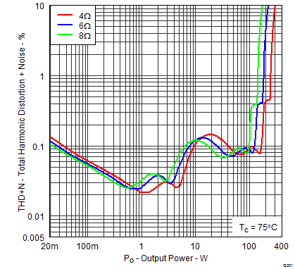 Figure 2. Total Harmonic + Noise vs Output Power
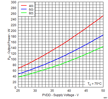 Figure 4. Unclipped Output Power vs Supply Voltage
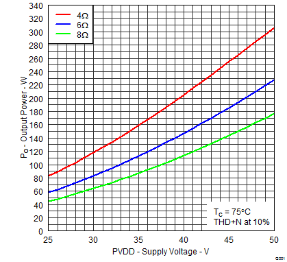 Figure 3. Output Power vs Supply Voltage
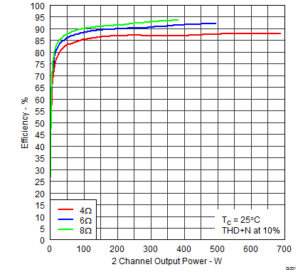 Figure 5. System Efficiency vs Output Power
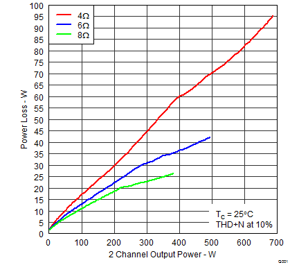 Figure 6. System Power Loss vs Output Power
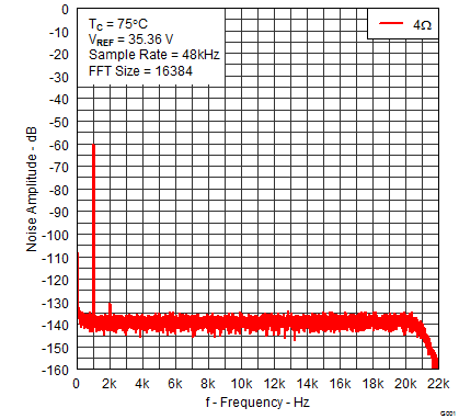 Figure 8. Noise Amplitude vs Frequency
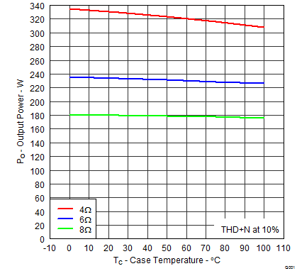 Figure 7. Output Power vs Case Temperature
6.9.2 SE Configuration
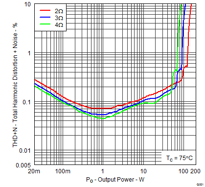 Figure 9. Total Harmonic Distortion + Noise vs Output Power
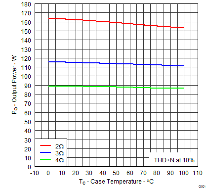 Figure 11. Output Power vs Case Temperature
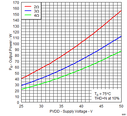 Figure 10. Output Power vs Supply Voltage
6.9.3 PBTL Configuration
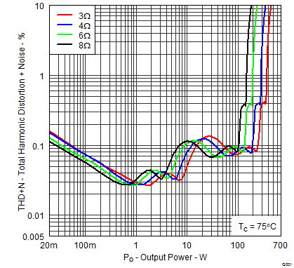 Figure 12. Total Harmonic Distortion + Noise vs Output Power
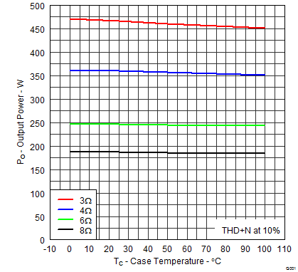 Figure 14. Output Power vs Case Temperature
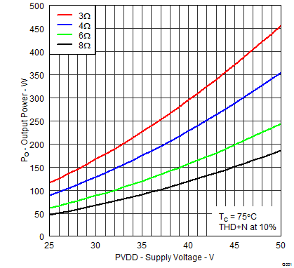 Figure 13. Output Power vs Supply Voltage