SBFS022C June 2003 – October 2015 SRC4192 , SRC4193
PRODUCTION DATA.
- 1 Features
- 2 Applications
- 3 Description
- 4 Revision History
- 5 Pin Configuration and Functions
- 6 Specifications
- 7 Detailed Description
- 8 Application and Implementation
- 9 Power Supply Recommendations
- 10Layout
- 11Device and Documentation Support
- 12Mechanical, Packaging, and Orderable Information
5 Pin Configuration and Functions
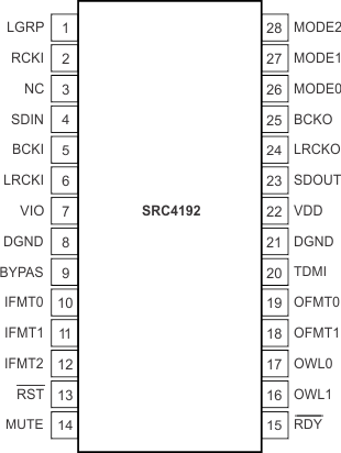
SRC4192 DB Package
28-Pin SSOP
Top View

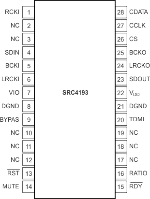
SRC4193 DB Package
28-Pin SSOP
Top View

Pin Functions
| PIN | I/O | DESCRIPTION | ||
|---|---|---|---|---|
| NAME | SRC4192 | SRC4193 | ||
| BCKI | 5 | 5 | I | Input port bit clock I/O |
| BCKO | 25 | 25 | O | Output port bit clock I/O |
| BYPAS | 9 | 9 | I | ASRC bypass control input (Active High) |
| CCLK | — | 27 | I | SPI port data clock input |
| CDATA | — | 28 | I | SPI port serial data input |
| CS | — | 26 | I | SPI port chip select input (Active Low) |
| DGND | 8, 21 | 8, 21 | – | Digital ground |
| IFMT0 | 10 | — | I | Input port data format control input |
| IFMT1 | 11 | — | I | Input port data format control input |
| IFMT2 | 12 | — | I | Input port data format control input |
| LGRP | 1 | — | I | Low group delay control input (active high) |
| LRCKI | 6 | 6 | I | Input port left/right word clock I/O |
| LRCKO | 24 | 24 | O | Output port left/right word clock I/O |
| MODE0 | 26 | — | I | Serial port mode control input |
| MODE1 | 27 | — | I | Serial port mode control input |
| MODE2 | 28 | — | I | Serial port mode control input |
| MUTE | 14 | 14 | I | Output mute control input (active high) |
| NC | 3 | 2,3,10,11,12,17,18,19 | – | No connection |
| OFMT0 | 19 | — | I | Output port data format control input |
| OFMT1 | 18 | — | I | Output port data format control input |
| OWL0 | 17 | — | I | Output port data word length control input |
| OWL1 | 16 | — | I | Output port data word length control input |
| RATIO | — | 16 | O |
Input-to-output ratio flag output Low output denotes output rate lower than input rate. High output denotes output rate higher than input rate. |
| RCKI | 2 | 1 | I | Reference Clock Input |
| RDY | 15 | 15 | O | ASRC Ready Status Output (Active Low) |
| RST | 13 | 13 | I | Reset Input (Active Low) |
| SDIN | 4 | 4 | I | Audio Serial Data Input |
| SDOUT | 23 | 23 | O | Audio Serial Data Output |
| TDMI | 20 | 20 | I | TDM Data Input (Connect to DGND when not in use) |
| VDD | 22 | 22 | I | Digital Core Supply, 3.3 V |
| VIO | 7 | 7 | I | Digital I/O Supply, 1.65 V to VDD |